
Introduction
At the heart of every microchip lies an extraordinary machine—the lithography machine. Often described as the “printing press” of the semiconductor industry, this system etches microscopic patterns onto silicon wafers, defining the transistors and circuits that power modern electronics. Without lithography, the smartphones in our pockets, AI supercomputers, and spacecraft electronics simply would not exist.
This article serves as a documentary-style tutorial, guiding you through the anatomy of a lithography machine, its working principles, and why it has become one of the most complex and expensive machines ever built.
1. What is Lithography?
Lithography in semiconductor manufacturing is a process of transferring circuit patterns onto a silicon wafer. Similar to how a projector casts an image onto a screen, lithography machines project a blueprint of electronic circuits onto a wafer coated with light-sensitive material (photoresist).
- Scale of operation: Nanometer precision (1 nm = 1 billionth of a meter).
- Key role: Defines chip density, speed, and energy efficiency.
- Industry significance: The smaller the patterns, the more transistors per chip (Moore’s Law).
2. Types of Lithography Machines
- Deep Ultraviolet Lithography (DUV): Uses 193 nm light (ArF laser).
- Extreme Ultraviolet Lithography (EUV): Uses 13.5 nm wavelength, enabling the most advanced chips (2–3 nm nodes).
- Legacy Optical Lithography: Older systems (248 nm, 365 nm) used in simpler chips and sensors.
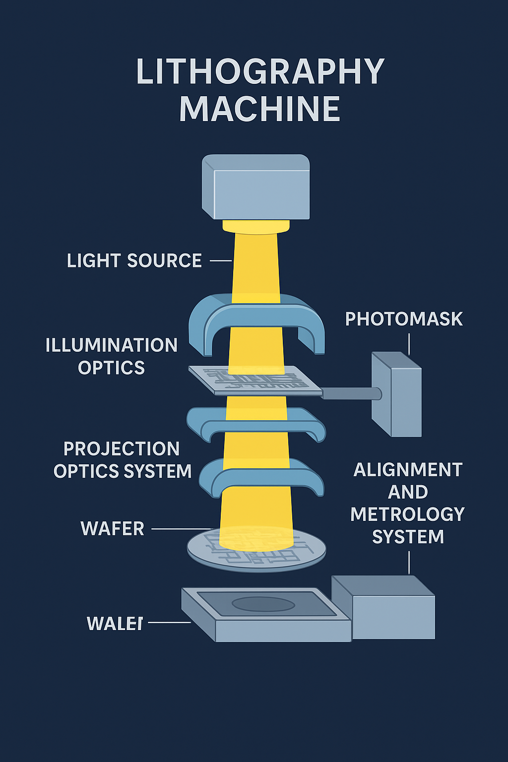
3. Anatomy of a Lithography Machine
A modern EUV lithography system, such as those built by ASML in the Netherlands, consists of several critical modules:
a) Light Source
- For EUV: Generated by firing high-energy laser pulses at molten tin droplets to create plasma that emits 13.5 nm EUV light.
- For DUV: Uses excimer lasers (ArF or KrF).
- Challenge: Extremely high brightness and stability are required for mass production.
b) Illumination Optics
- Shapes and conditions the light beam.
- Uses complex mirrors (in EUV, conventional glass lenses cannot be used, as EUV is absorbed by everything—even air).
- Operates in a vacuum environment to prevent light loss.
c) Photomask (Reticle)
- A master blueprint of the chip circuit pattern.
- In EUV systems, special reflective masks are used since transmissive glass masks do not work at such short wavelengths.
d) Projection Optics System (POS)
- Reduces the size of the pattern on the mask and projects it onto the wafer.
- Uses ultra-precise mirrors with atomic-scale smoothness (made by ZEISS in Germany).
- Ensures distortion-free imaging at nanometer resolution.
e) Wafer Stage
- Holds the silicon wafer.
- Moves at high speed with nanometer accuracy using magnetic levitation.
- Coordinates with the projection system to ensure patterns align perfectly across layers.
f) Photoresist and Coating System
- Wafer is coated with a thin layer of photoresist (light-sensitive polymer).
- When exposed to light, the resist chemically changes, allowing selective removal to form circuit pathways.
g) Alignment and Metrology Systems
- Real-time sensors ensure each layer aligns with nanometer precision.
- Corrects for thermal expansion, vibration, and stage motion errors.
4. Step-by-Step Lithography Process (Tutorial View)
- Coating: Wafer coated with photoresist.
- Alignment: Machine aligns wafer to the mask with sub-nm accuracy.
- Exposure: Light is projected through the photomask onto the wafer.
- Development: Exposed photoresist is chemically developed, revealing patterns.
- Etching / Implantation: The revealed wafer areas are etched or doped.
- Layering: Process repeats hundreds of times to build a complete chip.
5. Scale and Complexity
- EUV machine cost: ~$200 million each.
- Weight: ~180 tons, with 100,000+ precision parts.
- R&D Ecosystem: Only ASML makes EUV machines, supported by global suppliers (Zeiss optics, Cymer light sources, etc.).
- Precision benchmark: Accuracy within fractions of a nanometer—comparable to aiming a laser pointer at the moon and hitting a coin.
6. The Future of Lithography
- High-NA EUV (0.55 NA): Next-generation optics for 2 nm and below.
- Multi-patterning: Layering techniques to extend Moore’s Law.
- Beyond Lithography: Research into directed self-assembly, nanoimprint lithography, and quantum-level patterning.
Conclusion
The lithography machine is often described as “the most complicated machine ever made by humankind.” Its anatomy is a perfect marriage of physics, chemistry, optics, and precision engineering. For engineers, researchers, and technology enthusiasts, understanding lithography is like understanding the very DNA of modern electronics.
It is not just a machine—it is the invisible engine that drives the digital revolution.


Be First to Comment