
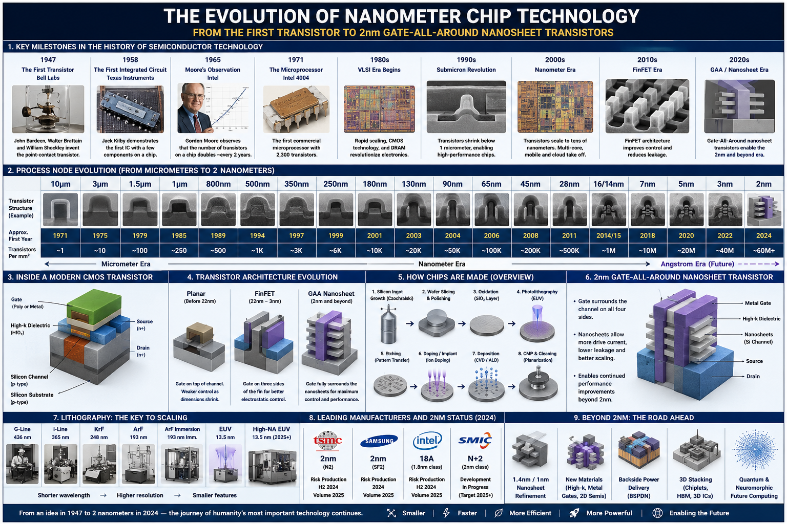
Invention, Anatomy, and History of Semiconductor Nanotechnology — From the First Transistor to the 2-Nanometer Node
Executive Summary
The nanometer chip is arguably the single most consequential artifact of the modern era. Fewer than eighty years separate the first crude point-contact transistor, assembled by hand at Bell Telephone Laboratories in December 1947, from today’s two-nanometer logic transistors, whose channels are built one atomic layer at a time and whose gates wrap fully around silicon sheets only a few dozen atoms thick.
Three threads run through this history: materials science (strained silicon, high-k dielectrics, nanosheet channels), geometry (planar → FinFET → gate-all-around → future CFET), and capital concentration, as fewer companies can afford the machines required to print a 2nm transistor.
Reading note
Figures for cost, yield, and production timing reflect the most recent public disclosures available as of mid-2026 and should be treated as industry estimates rather than audited figures. Copy Section
1 · What Is a Nanometer? Foundations of Scale
A nanometer is one billionth of a metre — a distance so small that a single strand of human hair, at roughly 80,000–100,000 nanometres wide, is tens of thousands of times thicker than the transistor features described here. A silicon atom itself spans roughly 0.2–0.3 nanometres, meaning a “2 nanometre” transistor feature is only about seven to ten atoms wide.
Since the FinFET era began in 2011, node names such as “7nm,” “3nm,” and “2nm” have described a generational marketing tier — density, performance, and power taken together — rather than a single literal measurement. A TSMC “2nm” transistor and a Samsung “2nm” transistor are not identical in dimension.
Why Smaller Is Better
Shrinking a transistor delivers three benefits simultaneously: faster switching, lower energy per switch, and more transistors per chip. This virtuous cycle was formalised in 1965 by Intel co-founder Gordon Moore, whose “Moore’s Law” is an industrial target the sector chose to hit repeatedly by inventing new physics whenever the old ran out of room.
Key figure
A modern 2nm-class chip can contain over 30 billion transistors on a piece of silicon smaller than a fingernail — roughly four times the transistor count of a leading 7nm chip from 2018. Copy Section
2 · The Birth of the Transistor, 1947–1959
The Point-Contact Transistor
On 16 December 1947, John Bardeen and Walter Brattain at Bell Labs demonstrated the first working transistor: a block of germanium with two gold contacts pressed into its surface, capable of amplifying an electrical signal — proof that a solid crystal could replace bulky, power-hungry vacuum tubes.
The Junction Transistor and Silicon
William Shockley developed the more robust junction transistor in 1948. Germanium dominated early production, but Texas Instruments’ Gordon Teal produced the first practical silicon transistor in 1954 — silicon’s stable oxide and thermal behaviour made it the industry’s lasting choice.
The Planar Process
In 1959, Jean Hoerni at Fairchild developed the planar process, growing a protective silicon dioxide layer directly on the wafer to make transistors flat, uniform, and reproducible via photographic patterning. Every chip made since — including 2026’s 2nm logic — descends directly from this process.
Historical note
Shockley, Bardeen, and Brattain shared the 1956 Nobel Prize in Physics for the transistor. Bardeen later won a second Nobel Prize in 1972 — the only person to win the Physics prize twice. Copy Section
3 · The Integrated Circuit and the Planar Process
By the late 1950s, computers required thousands of hand-wired components — “the tyranny of numbers.” Jack Kilby at Texas Instruments built the first working integrated circuit in September 1958; Robert Noyce at Fairchild, building on Hoerni’s planar process, developed the more manufacturable version in 1959 using printed metal traces instead of hand-wiring.
Kilby received the Nobel Prize in 2000; Noyce had already died and Nobel Prizes are not awarded posthumously. Noyce co-founded Intel with Gordon Moore in 1968. Intel’s 4004, released in 1971 on a ~10-micrometre process with 2,300 transistors, became the first commercial microprocessor — the direct ancestor of every chip since.
Perspective
The 4004’s 10-micrometre features were roughly 5,000 times larger than a modern 2nm feature. It held 2,300 transistors; a modern high-end GPU on a 2nm-class process can hold over 100 billion. Copy Section
4 · Moore’s Law and the March of the Micron Nodes
Between the early 1970s and early 2000s, the industry advanced through more than a dozen node generations, each roughly halving transistor area.
| Year | Node / Feature Size | Milestone |
|---|---|---|
| 1971 | 10 µm | Intel 4004 — first commercial microprocessor |
| 1985 | 1 µm | Intel 80386 |
| 1994 | 0.5 µm | Pentium era begins |
| 1999 | 0.25–0.18 µm | Copper interconnects go industry-wide |
| 2003 | 90 nm | Strained silicon enters production |
| 2008 | 45 nm | First high-k metal gate transistors |
| 2012 | 22 nm | First commercial FinFET (Intel Tri-Gate) |
The copper interconnect shift (1997–2002) and strained silicon (2003) rank among the era’s most important materials breakthroughs — both remain embedded in every leading-edge transistor made today. Copy Section
5 · The Deep Submicron Era: Strain, High-k, and Immersion Light
The Leakage Crisis
By the mid-2000s, silicon dioxide gates had thinned to a few atomic layers, causing quantum-tunnelling leakage. Intel’s 2007 fix at 45nm: a hafnium-based high-k dielectric paired with new metal gates, replacing decades-old polysilicon.
Immersion Lithography
To pattern features smaller than 193nm DUV light’s wavelength, engineers introduced immersion lithography around 2006 — a layer of purified water between lens and wafer, sharpening resolution. Combined with multi-patterning, it carried the industry from 45nm to 14–10nm.
Why multiple patterning was needed
Splitting one dense layer into several coarser exposures solved resolution but added huge cost — motivating the eventual shift to EUV lithography (Chapter 10). Copy Section
6 · The FinFET Revolution, 22nm to 5nm
Planar transistors suffered short-channel leakage as gates lost control over shrinking channels. Intel’s 2011 fix, commercialised at 22nm: stand the channel up as a thin “fin,” gated on three sides — the FinFET, the first fundamental geometry change since the planar process.
FinFETs became the standard for over a decade across 22, 14, 10, 7, and 5nm. TSMC’s 3nm node (2022) was the last major FinFET generation — fins had grown so tall and thin that a further architectural change became necessary.
| Node | Year | Leader | Note |
|---|---|---|---|
| 22 nm | 2012 | Intel | First commercial FinFET |
| 7 nm | 2018 | TSMC | First EUV insertion (select layers, 2019) |
| 5 nm | 2020 | TSMC | 170M+ transistors/mm² |
| 3 nm | 2022 | TSMC | Final major FinFET generation |
Copy Section
7 · The Gate-All-Around Transition at 3 Nanometers
The FinFET’s successor reshapes the channel again — into thin horizontal sheets stacked atop one another, gated on all four sides: the gate-all-around (GAA) nanosheet transistor, offering the greatest electrostatic control yet commercialised.
Samsung was first, branding its version MBCFET at 3nm (SF3) in 2022, though early yields lagged FinFET rivals. Much foundational research originated at IBM’s Albany NanoTech centre. TSMC deliberately extended FinFET one more generation before adopting nanosheets; Intel held its RibbonFET GAA design for its 20A/18A nodes. By 2024, all three leading manufacturers had committed to nanosheet GAA for the 2nm generation.
Why nanosheets, not just narrower fins
A fin is only ever gated from three sides. A nanosheet, gated from all four, gives markedly better control — and can be widened without enlarging the transistor’s footprint, enabling flexible “NanoFlex”-style design. Copy Section
8 · Anatomy of the 2-Nanometer Chip
The Nanosheet Transistor Channel
At the core: two to four thin horizontal silicon sheets per transistor, each a few nanometres thick, fully surrounded by a hafnium-based high-k gate stack — dramatically cutting off-state leakage versus even the best FinFETs, and enabling lower operating voltages.
NanoFlex and Cell-Level Flexibility
TSMC’s N2 introduces NanoFlex: variable nanosheet width without changing footprint, letting designers mix high-performance and power-efficient transistors within one standard cell library — a freedom FinFETs’ fixed fin geometry never offered.
Backside Power Delivery
Power wiring moves to the wafer’s reverse side, freeing the front for signal routing. Intel’s PowerVia shipped first on 18A (late 2025); TSMC’s Super Power Rail arrives on A16 (2H 2026) — one generation after N2’s initial GAA introduction.
SHPMIM Capacitors and Interconnects
N2 also introduces SHPMIM capacitors — roughly double the capacitance density, half the resistance — stabilising power to billions of switching transistors. More EUV exposures on a 2nm chip now go toward interconnects than the transistor layer itself.
| Attribute | Detail |
|---|---|
| Architecture | Gate-all-around stacked nanosheet, 2–4 sheets/device |
| Perf vs. N3E (iso-power) | 10%–15% faster |
| Power vs. N3E (iso-speed) | 25%–30% lower |
| Power delivery | Front-side at N2; backside from A16 (TSMC) / already on Intel 18A |
| Approx. wafer cost | ~USD 30,000 (industry estimate) |
Copy Section
9 · The Global 2nm Race: TSMC, Samsung, and Intel
TSMC N2
Volume production began Q4 2025 at Fab 22 (Kaohsiung), with Fab 20 (Hsinchu) following. Early yields around 70%, targeting ~80% for N2P (2H 2026). Capacity plans scale from ~40,000 wafers/month (late 2025) toward ~100,000 in 2026 and ~200,000 by 2027. Lead customers: Apple, AMD, Nvidia, Qualcomm.
Samsung SF2
Mass production began 2025 using MBCFET GAA, debuting in the Exynos 2600. Reported yields ~50–60% into early 2026; a refined SF2P variant is planned for 2026.
Intel 18A and the Angstrom Era
Intel skipped a conventional “2nm” label, advancing directly to 18A — combining RibbonFET GAA with PowerVia backside power from the first generation. Entered high-volume manufacturing in late 2025, serving both Intel products and external foundry customers.
A note on geopolitics
EUV tools come from a single supplier (ASML, Netherlands); export policy in the US, EU, Japan, and China now actively shapes the 2nm roadmap. This document does not take a policy position. Copy Section
10 · Manufacturing at the Atomic Frontier
Extreme Ultraviolet Lithography
EUV uses 13.5nm-wavelength light — reflected off ultra-precise mirrors rather than lenses, since EUV is absorbed by conventional glass. TSMC introduced it selectively at 7nm (2019), more broadly at 5/3nm, and it now underpins most critical N2 layers.
High-NA EUV: The Next Optical Leap
High-NA EUV raises numerical aperture from 0.33 to 0.55. ASML’s EXE:5000 resolves ~8nm features — ~1.7x smaller prints. As of mid-2026, adoption in 2nm-class volume manufacturing remains partial; broader use is planned for TSMC’s A14 and Intel’s 14A. Fewer than a dozen EXE:5200 systems exist worldwide, priced around €350–400 million each.
Atomic Layer Deposition
Every layer around a recessed 3D nanosheet must now be built with near-atomic precision — making atomic layer deposition (ALD) effectively mandatory for gate stacks at this scale.
Yield, Cost, and Economics
A 2nm-class wafer costs an estimated ~USD 30,000 — several times an equivalent wafer two generations earlier — explaining why only TSMC, Samsung, and Intel, alongside a narrow equipment-supplier base, can compete at the leading edge. Copy Section
11 · Beyond 2 Nanometers: The Roadmap to 2030
N2P, N2X, A16 — N2P (2H 2026) refines power/performance without backside power; A16 (2H 2026) combines nanosheet GAA with TSMC’s Super Power Rail for AI/HPC processors.
A14 and A12 — second-generation nanosheet GAA with enhanced NanoFlex Pro, extending the family through the rest of the decade.
Intel 14A and Samsung SF2P — Intel’s first High-NA EUV node (~2027); Samsung’s refined second-generation 2nm process ramping in 2026.
Complementary FET and Vertical Stacking
IBM and imec are developing the CFET, stacking a logic gate’s two transistor types vertically to roughly halve area. A related “nanostack” direction extends 3D integration further via hybrid wafer bonding; IBM’s informal “0.7nm”-class label describes a roadmap ambition, not a qualified process — production proof points, including from Japan’s Rapidus consortium, are expected toward decade’s end.
A grounded caveat
Names like “1.4nm,” “A12,” or “0.7nm” describe marketing generations, not literal dimensions. Every node in this chapter remains, as of mid-2026, at the roadmap or early-development stage. Copy Section
12 · Implications and Conclusion
The path from Bardeen and Brattain’s 1947 point-contact transistor to 2026’s gate-all-around nanosheets spans not quite eighty years, yet compresses an extraordinary density of breakthroughs — the planar process, the integrated circuit, strained silicon, high-k metal gates, immersion lithography, the FinFET, EUV, and now nanosheets and backside power. No single insight carried the industry the whole distance.
Three practical implications follow: leading-edge manufacturing now functions as a natural oligopoly; performance gains increasingly come from architecture and system integration rather than the node number alone; and geographic concentration of equipment supply and manufacturing makes supply security a permanent structural feature of the industry, not a temporary disruption.
The nanometer chip is not a finished invention — it is a continuously renegotiated compromise between physics, materials science, and economics, sustained across roughly seventeen major node generations since 1971. Copy Section
Glossary of Key Terms
NodeAn industry generation label, not a literal physical measurement since the FinFET era. FinFETA transistor with a standing, three-sided-gated “fin” channel; dominant 2012–~2022. Gate-all-around (GAA) / nanosheetGate fully surrounds one or more horizontal channel sheets; succeeds FinFET from ~3–2nm. High-k metal gateHafnium-based high-dielectric gate stack with metal electrodes, introduced 2007. Strained siliconLattice deliberately stretched/compressed to improve carrier mobility; introduced at 90nm, 2003. EUV lithography13.5nm-wavelength light with reflective optics, patterning the finest circuit layers. High-NA EUVEUV tool generation with 0.55 numerical aperture, resolving finer features than 0.33 NA systems. Backside power deliveryPower wiring moved to the wafer’s reverse side; branded PowerVia (Intel), Super Power Rail (TSMC). Atomic layer deposition (ALD)Depositing material one atomic layer at a time for uniform 3D nanosheet coating. CFETFuture architecture stacking a logic gate’s two transistor types vertically to save area.






Be First to Comment