
Introduction
A graphics processing unit (GPU) represents one of the most complex and fascinating pieces of modern computing hardware. Unlike a CPU designed for sequential processing, a GPU is purpose-built for massive parallel computation, making it ideal for rendering graphics, scientific simulations, machine learning, and cryptocurrency mining. This comprehensive guide explores every aspect of GPU architecture, from physical construction to how data flows through the processing pipeline.
Physical Construction and Manufacturing
Silicon Substrate and Die Design
The heart of any graphics card is the GPU die—a rectangular piece of silicon containing billions of transistors. Modern GPUs like NVIDIA’s Ada Lovelace or AMD’s RDNA 3 architectures contain between 20 to 76 billion transistors fabricated using advanced processes ranging from 4nm to 5nm technology.
The manufacturing process begins with purified silicon wafers, typically 300mm in diameter. Through photolithography, circuit patterns are etched onto the wafer using ultraviolet light and photoresist chemicals. This process repeats dozens of times to build up the multiple layers of transistors, interconnects, and memory circuits. Each wafer contains dozens of GPU dies, which are later separated, tested, and packaged.
GPU Package and Substrate
Once the silicon die is fabricated, it must be mounted onto a substrate—a sophisticated printed circuit board that provides electrical connections between the die and the rest of the graphics card. Modern GPUs use advanced packaging techniques:
- Flip-chip bonding: The die is mounted upside down with microscopic solder bumps connecting directly to the substrate
- Interposer technology: High-end GPUs use silicon interposers that sit between the GPU die and substrate, enabling extremely high-bandwidth connections to memory chips
- Multi-chip modules: Recent designs like AMD’s chiplet architecture separate the GPU into multiple dies connected through advanced packaging
The package also includes a heat spreader—typically copper or nickel-plated copper—that distributes heat from the die to the cooling solution.
Core GPU Architecture Components
Streaming Multiprocessors (SMs) / Compute Units (CUs)
The fundamental building block of GPU computation is the streaming multiprocessor (NVIDIA terminology) or compute unit (AMD terminology). A modern gaming GPU contains anywhere from 20 to 140+ of these units.
Each SM/CU contains:
CUDA Cores / Stream Processors: The individual arithmetic logic units (ALUs) that perform calculations. A single SM might contain 64-128 CUDA cores. Each core can execute one floating-point or integer operation per clock cycle.
Tensor Cores / Matrix Engines: Specialized units introduced for AI and deep learning workloads. These can perform multiple multiply-accumulate operations simultaneously, offering 8-16x the throughput of standard cores for matrix mathematics.
Ray Tracing Cores / Ray Accelerators: Dedicated hardware for calculating ray-triangle intersections and bounding volume hierarchy (BVH) traversal, essential for real-time ray tracing in modern games.
Special Function Units (SFUs): Handle complex mathematical operations like sine, cosine, logarithms, and reciprocal calculations.
Load/Store Units (LSUs): Manage memory access operations, moving data between registers and various memory hierarchies.
Memory Hierarchy
GPUs employ a sophisticated multi-level memory system designed to feed thousands of parallel processing units:
Registers: The fastest storage, located directly within each SM. Modern GPUs have tens of thousands of 32-bit registers per SM, providing immediate access for actively executing threads.
L1 Cache / Shared Memory: Each SM has 64-128 KB of extremely fast cache memory. Programmers can manually manage portions of this as “shared memory” for cooperative thread operations, or let the GPU use it automatically as L1 cache.
L2 Cache: A unified cache shared across all SMs, typically ranging from 4 MB to 96 MB in modern GPUs. The L2 cache significantly reduces trips to slower VRAM.
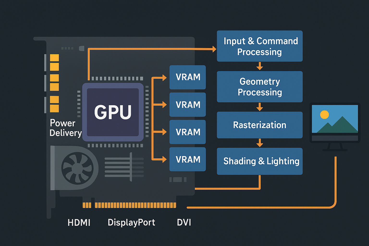
VRAM (Video Random Access Memory): The main graphics memory, ranging from 4 GB in budget cards to 24 GB or more in professional models. Modern cards use GDDR6 or GDDR6X memory, offering bandwidth exceeding 1 TB/s through wide 256-bit to 384-bit memory buses.
System RAM: Through PCIe, GPUs can access system memory, though at much lower speeds (16-32 GB/s vs 500+ GB/s for VRAM).
Rasterization and Graphics Pipeline Hardware
Beyond compute capabilities, GPUs contain specialized fixed-function hardware for graphics:
Raster Engines: Convert geometric primitives (triangles) into pixels, determining which pixels fall within each triangle’s boundaries.
Texture Units: Sample texture data from memory and apply filtering algorithms (bilinear, trilinear, anisotropic) to create smooth surface details.
Render Output Units (ROPs): Handle the final stages of rendering—depth testing, blending, anti-aliasing, and writing final pixel colors to the framebuffer.
Geometry Engines: Process vertex data, handle tessellation, and manage the geometry pipeline stages.
The Graphics Rendering Pipeline
Stage 1: Input Assembly and Vertex Processing
When a game or application wants to render a 3D scene, it sends draw commands to the GPU. The process begins with vertex data—3D coordinates, colors, texture coordinates, and normals for each vertex in the scene’s geometry.
Input Assembly: The GPU fetches vertex and index data from VRAM. Index buffers allow vertices to be reused across multiple triangles, reducing memory usage.
Vertex Shader Execution: Each vertex is processed by a vertex shader program—a small program that transforms vertex positions from object space to screen space. This involves:
- Model transformation (object to world space)
- View transformation (world to camera space)
- Projection transformation (camera to screen space)
Vertex shaders also calculate per-vertex lighting, pass texture coordinates to later stages, and can perform deformations like skeletal animation or cloth simulation.
Modern GPUs execute vertex shaders on their compute cores, processing thousands of vertices in parallel across multiple SMs.
Stage 2: Tessellation (Optional)
For games using tessellation, additional stages subdivide geometry to add detail:
Hull Shader: Determines how much to subdivide each patch of geometry based on factors like distance from camera.
Tessellator: A fixed-function unit that generates new vertices according to the hull shader’s instructions.
Domain Shader: Positions the newly generated vertices, applying displacement maps to create detailed surface geometry.
This process can transform a simple low-polygon mesh into millions of triangles, creating realistic terrain, characters, and objects.
Stage 3: Geometry Processing
Geometry Shader (optional): Can generate, modify, or discard entire primitives. Used for effects like particle generation, shadow volume extrusion, or creating fur/grass from single points.
Viewport Transformation: Triangles are scaled and positioned to match the output resolution.
Culling: Back-face culling removes triangles facing away from the camera. View frustum culling discards triangles completely outside the visible area.
Stage 4: Rasterization
The rasterization stage converts geometric primitives into pixels (fragments):
Triangle Setup: Calculate edge equations that define triangle boundaries.
Scan Conversion: Determine which pixels are covered by each triangle. The rasterizer generates a fragment for each covered pixel, interpolating vertex attributes (colors, texture coordinates, normals) across the triangle’s surface using barycentric coordinates.
Early Depth Testing: Before expensive pixel shading, the GPU can check if fragments will be occluded by previously rendered geometry, discarding them immediately to save processing.
Stage 5: Pixel/Fragment Shading
This is often the most computationally intensive stage. Each fragment runs through a pixel shader program that calculates its final color:
Texture Sampling: The shader reads texture data through texture units. For a single pixel, multiple texture samples might be needed:
- Mip-mapping selects appropriate detail levels based on distance
- Anisotropic filtering samples along the viewing angle for sharp textures on angled surfaces
- Trilinear filtering blends between mip levels for smooth transitions
Lighting Calculations: Complex lighting models calculate how light interacts with surfaces:
- Diffuse lighting (Lambertian reflectance)
- Specular highlights (Phong, Blinn-Phong, or physically-based models)
- Normal mapping for detailed surface features
- Environment mapping for reflections
Material Properties: Physically-based rendering (PBR) uses parameters like metalness, roughness, and albedo to simulate realistic material appearance.
Advanced Effects: Modern pixel shaders handle screen-space reflections, ambient occlusion, fog, color grading, and numerous other effects.
Pixel shaders execute on CUDA cores/stream processors, with warps/wavefronts of 32-64 pixels processed together for efficiency.
Stage 6: Ray Tracing (Modern GPUs)
Ray tracing GPUs integrate real-time ray tracing into the pipeline:
Ray Generation: Rays are cast from the camera through each pixel into the scene.
BVH Traversal: Ray tracing cores traverse acceleration structures (bounding volume hierarchies) to quickly determine which geometry each ray might intersect.
Intersection Testing: Specialized hardware tests ray-triangle intersections at billions per second.
Shading: When a ray hits a surface, a shader calculates the color, potentially casting additional rays for reflections, refractions, and shadows.
Denoising: Because full ray tracing is still expensive, GPUs trace fewer rays and use AI-accelerated denoising algorithms (running on tensor cores) to reconstruct clean images.
Stage 7: Output Merger and Display
Depth Testing: Fragments are compared against the depth buffer (Z-buffer) to determine if they’re in front of previously rendered geometry.
Stencil Testing: Uses a stencil buffer for techniques like portal rendering, outlining, or shadow volumes.
Blending: For transparent objects, fragment colors are blended with colors already in the framebuffer using various equations (alpha blending, additive, multiplicative).
Anti-Aliasing: ROPs apply techniques to reduce jagged edges:
- MSAA (Multisample Anti-Aliasing): Samples multiple points per pixel
- TAA (Temporal Anti-Aliasing): Uses information from previous frames
- FXAA/SMAA: Post-processing approaches
Framebuffer Write: Final pixel colors are written to VRAM in the framebuffer.
Display Output: The display controller reads the framebuffer and sends pixel data through display connectors (HDMI, DisplayPort) to the monitor, synchronized with refresh rates via V-Sync, G-Sync, or FreeSync.
Parallel Execution Model
Warps and Wavefronts
GPUs achieve massive parallelism through SIMT (Single Instruction, Multiple Thread) execution:
Threads are grouped into warps (NVIDIA, 32 threads) or wavefronts (AMD, 32-64 threads). All threads in a warp execute the same instruction simultaneously on different data.
Occupancy: SMs can have multiple warps in flight simultaneously (often 32-64 warps per SM). When one warp stalls waiting for memory, the SM immediately switches to another warp, hiding latency and keeping cores busy.
Thread Divergence
When threads in a warp take different code paths (if/else branches), the GPU must execute both paths serially, masking out threads not taking each path. This “divergence” reduces efficiency, so shader programmers try to minimize branching or ensure threads in a warp take the same branches.
Memory Coalescing
For maximum memory bandwidth, threads in a warp should access contiguous memory addresses. The GPU can combine these into a single wide memory transaction. Scattered, random access patterns cause multiple transactions, reducing performance.
Power Delivery and Thermal Management
Voltage Regulation Modules (VRMs)
Graphics cards convert the 12V power from PCIe slots and power connectors into the lower voltages (0.8V-1.2V) GPUs require. The VRM consists of:
MOSFETs: Transistors that switch power on and off thousands of times per second.
Inductors: Store energy and smooth voltage delivery.
Capacitors: Filter voltage fluctuations and provide stable power.
High-end cards use 10-20+ power phases for clean, stable power delivery under varying loads. Each phase can deliver 40-60 amps, with total power consumption reaching 300-450W for flagship models.
Cooling Systems
Modern GPUs generate enormous heat that must be dissipated:
Vapor Chamber / Heat Pipes: Copper structures filled with working fluid that evaporates at the GPU, carrying heat to cooler areas where it condenses.
Heatsink: Large aluminum or copper fin arrays maximize surface area for heat dissipation.
Fans: Two to three fans push air through the heatsink. Modern designs use dual ball bearings for longevity and optimize blade design for airflow vs. noise.
Thermal Interface Material (TIM): High-performance thermal paste or thermal pads conduct heat from the GPU die and memory chips to the cooler.
Backplate: A metal backplate provides structural support and helps dissipate heat from PCB components.
High-end cards may feature active cooling for VRMs and memory, RGB lighting systems, and sophisticated fan control that stops fans entirely at low loads (zero RPM mode).
Modern GPU Features and Technologies
DLSS and FSR (AI Upscaling)
Deep Learning Super Sampling (DLSS): NVIDIA’s tensor cores run neural networks trained on high-resolution images to upscale lower-resolution renders, delivering near-native quality at much higher framerates.
FidelityFX Super Resolution (FSR): AMD’s spatial and temporal upscaling techniques work across various GPU brands without specialized hardware.
DirectStorage and GPU Decompression
Modern APIs allow GPUs to decompress game assets directly from SSDs, bypassing CPU bottlenecks and enabling faster load times and streaming of high-quality textures.
Mesh Shaders
Replace the traditional vertex/geometry pipeline with more flexible compute-like shaders that process entire meshlets, offering better culling and level-of-detail control.
Variable Rate Shading (VRS)
Allows games to shade different screen regions at different rates—full resolution where detail matters, lower resolution in peripheral vision or motion-blurred areas—improving performance without noticeable quality loss.
Compute Applications Beyond Graphics
GPGPU (General Purpose GPU Computing)
Modern GPUs excel at non-graphics tasks:
Scientific Computing: Protein folding, climate modeling, fluid dynamics simulations leverage thousands of parallel cores.
Machine Learning: Training neural networks involves massive matrix operations—perfect for GPU tensor cores. Training times reduced from months to days.
Cryptocurrency Mining: Parallel hash calculations for proof-of-work algorithms.
Video Encoding: Dedicated encoding engines (NVENC, VCE) handle H.264, H.265, and AV1 compression with minimal CPU usage.
3D Rendering: Production rendering engines like Octane, Redshift, and Cycles offload work from CPU to GPU, reducing render times by 10-100x.
Programming frameworks like CUDA (NVIDIA), ROCm (AMD), OpenCL, and Vulkan Compute enable developers to harness GPU power for any parallelizable task.
Performance Metrics and Bottlenecks
Key Specifications
TFLOPS (Tera Floating-Point Operations Per Second): Raw computational throughput. A modern GPU might deliver 20-80 TFLOPS.
Memory Bandwidth: How fast data moves between VRAM and GPU. Modern cards: 400-1000+ GB/s.
Pixel Fillrate: Pixels the ROPs can output per second. Calculated as: ROPs × Clock Speed.
Texture Fillrate: Texels the texture units can sample per second.
RT Performance: Ray tracing throughput measured in gigarays per second.
Common Bottlenecks
Memory Bandwidth Limitation: High-resolution textures and framebuffers can saturate memory bandwidth, especially at 4K resolution.
Compute Limitation: Complex shaders with heavy calculations can max out CUDA cores/stream processors.
ROP Limitation: High refresh rates with anti-aliasing can bottleneck the render output units.
PCIe Bandwidth: Transferring large amounts of data between system RAM and VRAM can become a bottleneck, though less common in gaming.
Future Directions
Chiplet Architectures
Following CPU trends, GPUs are moving toward chiplet designs—multiple smaller dies connected via advanced packaging. This improves yields, allows mixing different process nodes, and enables more flexible scaling.
Advanced AI Integration
Future GPUs will integrate more sophisticated AI accelerators for real-time path tracing denoising, upscaling, frame generation, and even AI-driven procedural content generation.
MCM (Multi-Chip Module) Scaling
Connecting multiple GPU dies to scale performance beyond single-die limitations, similar to AMD’s RDNA 3 architecture or Intel’s Ponte Vecchio.
Photonic Interconnects
Research into optical data transmission promises dramatically higher bandwidth between chiplets and memory while reducing power consumption.
Conclusion
Modern graphics cards represent the pinnacle of parallel computing architecture. From billions of transistors working in concert to render realistic 3D worlds at hundreds of frames per second, to the sophisticated memory hierarchies that feed insatiable compute demands, GPUs continue pushing the boundaries of what’s possible in real-time computing.
Understanding GPU architecture—from silicon fabrication through the rendering pipeline to final display output—reveals the extraordinary engineering that powers modern gaming, content creation, scientific research, and artificial intelligence. As demands for performance grow and new technologies emerge, GPU architecture will continue evolving, delivering ever more impressive capabilities to users worldwide.


Be First to Comment