Introduction
The semiconductor industry is the foundation of the modern digital world. Every smartphone, computer, automobile, medical device, industrial robot, artificial intelligence system, satellite, and communication network depends on semiconductor technologies. Semiconductors have become the “new oil” of the digital economy because they power innovation, economic growth, scientific discovery, and national security.
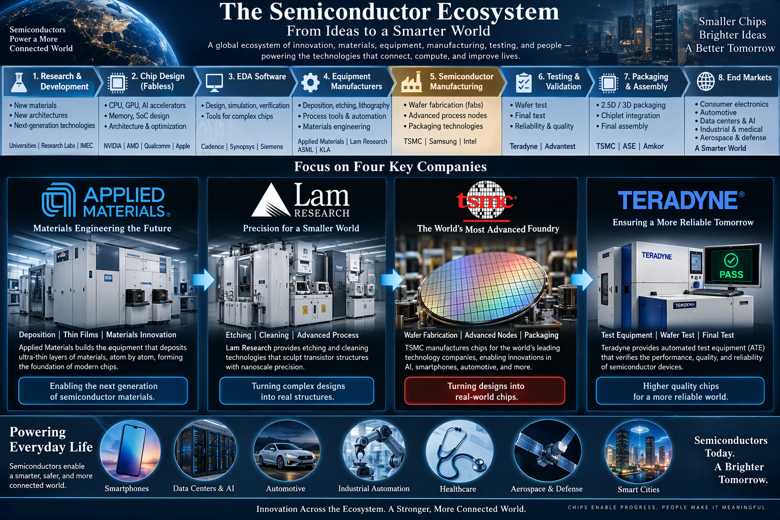
The semiconductor ecosystem is highly complex and consists of thousands of companies working together through design, manufacturing, equipment production, testing, packaging, materials supply, software development, and distribution. No single company controls the entire ecosystem. Instead, the industry’s success depends on collaboration between specialized firms.
Among the most important companies in this ecosystem are:
- Taiwan Semiconductor Manufacturing Company (TSMC)
- Applied Materials
- Lam Research
- Teradyne
These four companies represent critical pillars of semiconductor production and technological advancement. Together they enable the creation of the world’s most advanced microchips.
Chapter 1: Understanding the Semiconductor Ecosystem
What Is a Semiconductor?
A semiconductor is a material whose electrical conductivity lies between that of a conductor and an insulator.
Common semiconductor materials include:
- Silicon (Si)
- Gallium Arsenide (GaAs)
- Silicon Carbide (SiC)
- Gallium Nitride (GaN)
- Germanium (Ge)
Silicon remains the dominant semiconductor material because:
- It is abundant.
- It is cost effective.
- It offers excellent electrical properties.
- It can be manufactured at massive scale.
Modern semiconductor chips contain billions of transistors interconnected on a single piece of silicon.
Chapter 2: Architecture of the Semiconductor Ecosystem
The semiconductor ecosystem can be divided into several layers.
Layer 1: Research and Development
Universities, laboratories, and technology institutes create:
- New materials
- Advanced lithography techniques
- Novel transistor architectures
- Quantum computing concepts
- AI chip frameworks
Examples:
- MIT
- Stanford University
- IMEC
- TSMC Research Labs
Layer 2: Chip Design
Chip design companies create integrated circuits.
Examples:
- NVIDIA
- AMD
- Qualcomm
- Broadcom
- Apple
Design activities include:
- Processor architecture
- Memory design
- AI accelerator design
- Circuit optimization
These companies often do not manufacture chips themselves.
Layer 3: Electronic Design Automation (EDA)
EDA software is used to design chips.
Major EDA companies:
- Cadence
- Synopsys
- Siemens EDA
These tools help engineers design chips with billions of transistors.
Layer 4: Semiconductor Manufacturing
This layer converts chip designs into physical silicon devices.
The global leader:
TSMC
TSMC manufactures chips for:
- Apple
- NVIDIA
- AMD
- Qualcomm
- Broadcom
- MediaTek
TSMC is the world’s most advanced semiconductor foundry.
Layer 5: Equipment Manufacturers
Equipment suppliers build machines needed to produce semiconductors.
Examples:
- Applied Materials
- Lam Research
- ASML
- KLA
These companies create the sophisticated equipment necessary for wafer fabrication.
Layer 6: Testing and Validation
After manufacturing, chips must be tested.
Major companies include:
- Teradyne
- Advantest
Testing ensures:
- Reliability
- Performance
- Quality
Layer 7: Packaging and Assembly
Advanced packaging technologies include:
- 2.5D Packaging
- 3D Packaging
- Chiplet Architectures
Key companies:
- TSMC
- ASE Group
- Amkor
Chapter 3: TSMC – The Manufacturing Giant
Company Overview
Founded in 1987, Taiwan Semiconductor Manufacturing Company (TSMC) pioneered the pure-play foundry business model.
TSMC focuses solely on manufacturing chips designed by customers.
This revolutionary model allowed thousands of fabless chip companies to emerge.
Business Architecture
Inputs
TSMC receives:
- Chip designs
- Manufacturing specifications
- Process requirements
Processing
TSMC performs:
- Wafer fabrication
- Lithography
- Deposition
- Etching
- Packaging
Outputs
TSMC delivers:
- CPUs
- GPUs
- AI accelerators
- Mobile processors
- Automotive chips
Why TSMC Matters
Without TSMC:
- Apple iPhones would not exist in their current form.
- NVIDIA AI chips could not be mass produced.
- Modern cloud computing would be severely impacted.
TSMC’s significance includes:
1. Technology Leadership
Produces advanced nodes:
- 5nm
- 3nm
- 2nm technologies
2. Global Innovation Enabler
Provides manufacturing for:
- AI
- High-performance computing
- Smartphones
- Autonomous vehicles
3. Economic Impact
Generates hundreds of billions of dollars in economic value through technology production.
Chapter 4: Applied Materials – The Materials Engineering Leader
Company Overview
Applied Materials is one of the world’s largest semiconductor equipment manufacturers.
The company develops technologies used to build semiconductor devices atom by atom.
Core Technologies
Applied Materials specializes in:
Deposition
Deposits ultra-thin layers of materials onto silicon wafers.
Examples:
- Copper
- Tungsten
- Silicon nitride
- Dielectrics
Chemical Vapor Deposition (CVD)
Creates thin films essential for transistor construction.
Physical Vapor Deposition (PVD)
Used in metal interconnect formation.
Materials Engineering
Develops novel materials to improve:
- Performance
- Power efficiency
- Reliability
Significance of Applied Materials
1. Foundation of Transistor Manufacturing
Without advanced deposition systems, modern chips cannot be built.
2. Enables Miniaturization
Supports shrinking transistor dimensions.
3. Increases Yield
Improves manufacturing efficiency and reduces defects.
4. Accelerates Moore’s Law
Supports continued transistor scaling.
Chapter 5: Lam Research – The Etching Specialist
Company Overview
Lam Research is a world leader in wafer fabrication equipment.
Its expertise centers on:
- Etching
- Cleaning
- Deposition technologies
Understanding Etching
Etching removes unwanted material from silicon wafers.
Think of it as semiconductor sculpture.
The process carves:
- Gates
- Trenches
- Interconnects
- Memory cells
at nanoscale precision.
Lam Research Technologies
Plasma Etching
Uses ionized gases to remove material.
Advantages:
- Extreme precision
- High selectivity
- Uniformity
Atomic Layer Etching
Removes material one atomic layer at a time.
Required for:
- 3nm
- 2nm
- Future process nodes
Wafer Cleaning
Removes:
- Particles
- Contaminants
- Chemical residue
Why Lam Research Matters
1. Precision Manufacturing
Allows creation of microscopic transistor structures.
2. Advanced Memory Production
Critical for NAND and DRAM fabrication.
3. AI Chip Manufacturing
Supports production of high-density AI processors.
4. Yield Improvement
Enhances semiconductor production efficiency.
Chapter 6: Teradyne – The Quality Assurance Leader
Company Overview
Teradyne is a global leader in automated test equipment (ATE).
It verifies the performance of semiconductor devices before shipment.
Why Testing Is Critical
A chip containing billions of transistors can fail because of a tiny defect.
Testing ensures:
- Reliability
- Safety
- Functionality
Without testing, defective chips could enter:
- Data centers
- Medical systems
- Vehicles
- Aircraft
Teradyne’s Solutions
Wafer Testing
Checks chips before packaging.
Final Testing
Ensures chips perform correctly after packaging.
System-on-Chip Testing
Validates:
- CPU functionality
- GPU functionality
- AI accelerator performance
Teradyne’s Importance
1. Customer Trust
Guarantees product quality.
2. Reduced Failure Rates
Protects manufacturers from costly defects.
3. Supports AI Chip Validation
Tests increasingly complex AI processors.
4. Improves Supply Chain Reliability
Maintains confidence across global markets.
Chapter 7: How These Four Companies Work Together
The semiconductor manufacturing chain can be visualized as follows:
Step 1
Chip designers create architectures.
Examples:
- NVIDIA
- AMD
- Apple
↓
Step 2
Applied Materials equipment deposits atomic layers necessary to construct transistors.
↓
Step 3
Lam Research equipment etches transistor structures with nanoscale precision.
↓
Step 4
TSMC manufactures complete semiconductor wafers.
↓
Step 5
Teradyne tests chips for performance and quality.
↓
Step 6
Finished chips enter products worldwide.
Chapter 8: Impact on Artificial Intelligence
AI has increased semiconductor importance dramatically.
AI systems require:
- Massive computing power
- High-speed memory
- Advanced GPUs
- Efficient data movement
The four companies contribute as follows:
TSMC
Manufactures AI chips.
Applied Materials
Creates materials and deposition technologies.
Lam Research
Provides precision etching equipment.
Teradyne
Ensures AI chips function correctly.
Together they form a critical AI infrastructure ecosystem.
Chapter 9: Economic and Geopolitical Significance
Semiconductors influence:
- National security
- Economic competitiveness
- Technological leadership
The semiconductor ecosystem has become strategically important for:
- United States
- Taiwan
- China
- Europe
- Japan
- South Korea
These nations invest billions in semiconductor capabilities.
Chapter 10: Future of the Semiconductor Ecosystem
Emerging trends include:
Artificial Intelligence Chips
Rapid growth in AI accelerators.
2nm and Beyond
Smaller transistors enabling greater performance.
Advanced Packaging
Chiplet-based architectures.
Quantum Computing
Next-generation computational systems.
Autonomous Vehicles
Increasing semiconductor content per vehicle.
Edge Computing
Distributed AI processing.
Sustainable Manufacturing
Reducing energy and environmental impact.
Conclusion
The semiconductor ecosystem is one of the most sophisticated industrial systems ever created. It combines materials science, physics, engineering, software, automation, and global manufacturing into a tightly interconnected network. Within this ecosystem, TSMC, Applied Materials, Lam Research, and Teradyne occupy unique and irreplaceable positions.
TSMC transforms designs into advanced silicon chips. Applied Materials provides the materials engineering technologies that make semiconductor manufacturing possible. Lam Research delivers the precision etching and cleaning systems needed to create nanoscale transistor structures. Teradyne ensures final products meet rigorous quality and reliability standards.
Together, these four companies form a foundational architecture that supports the entire digital economy. Their collective contributions drive artificial intelligence, cloud computing, smartphones, automotive electronics, medical technologies, industrial automation, and future innovations. As technology advances toward AI-driven societies, quantum computing, and autonomous systems, the importance of these companies and the broader semiconductor ecosystem will continue to grow, shaping the future of the global economy and human progress.




Be First to Comment