Introduction: The Most Complex Machines Ever Built
Extreme Ultraviolet (EUV) lithography represents one of humanity’s most extraordinary technological achievements. These machines, which cost approximately $200-400 million each and weigh around 180 tons, are essential for manufacturing the most advanced semiconductor chips that power everything from smartphones to artificial intelligence systems. Yet despite their critical importance to the global economy, only one company in the world can manufacture them: ASML Holding NV of the Netherlands.
This article explores the intricate supply chain behind EUV machines, the chip foundries that depend on them, their subsidiary operations worldwide, and the complex web of clients that drive demand for cutting-edge semiconductors.
Understanding EUV Lithography Technology
EUV lithography uses light with a wavelength of 13.5 nanometers—roughly 40 times shorter than the deep ultraviolet (DUV) light used in previous generation lithography systems. This extremely short wavelength enables the printing of features as small as 7 nanometers and below on silicon wafers, making it possible to pack billions of transistors onto a single chip.
The technology works by generating EUV light through a process called laser-produced plasma. Tiny droplets of molten tin are fired at 50,000 times per second and struck mid-air by a high-powered laser, creating a plasma that emits EUV light. This light is then directed through a series of highly reflective mirrors to project circuit patterns onto silicon wafers coated with photoresist.
The extreme precision required is staggering: if an EUV mirror were scaled to the size of Germany, the largest imperfection would be less than a millimeter high. The entire system must operate in a near-perfect vacuum because EUV light is absorbed by virtually everything, including air.
ASML: The Sole Monopoly on EUV Technology
Corporate Structure and Operations
ASML Holding NV, headquartered in Veldhoven, Netherlands, stands as the only manufacturer of EUV lithography systems in the world. Founded in 1984 as a joint venture between Philips and Advanced Semiconductor Materials International (ASMI), ASML has evolved into one of Europe’s most valuable technology companies, with a market capitalization exceeding $300 billion at its peak.
The company’s monopoly on EUV technology stems from decades of research, development, and over $9 billion in investment. ASML’s current flagship products include:
- TWINSCAN NXE:3600D: The latest generation EUV system with throughput of 160 wafers per hour
- TWINSCAN NXE:3400C: Previous generation with 140-145 wafers per hour capability
- High-NA EUV systems: Next-generation machines capable of 0.55 numerical aperture, enabling sub-3nm manufacturing
Global Footprint
ASML operates through a global network of facilities:
Research & Development Centers:
- Veldhoven, Netherlands (headquarters and primary R&D)
- San Diego, California, USA (applications and customer support)
- Wilton, Connecticut, USA (optics development)
- Chandler, Arizona, USA
- Berlin, Germany
- Linkou, Taiwan
Manufacturing Sites:
- Veldhoven, Netherlands (final assembly)
- Wilton, Connecticut, USA (DUV systems and components)
- South Korea (customer support and services)
Regional Offices:
- Over 60 locations across 16 countries including Japan, China, Taiwan, South Korea, Singapore, Israel, and throughout Europe
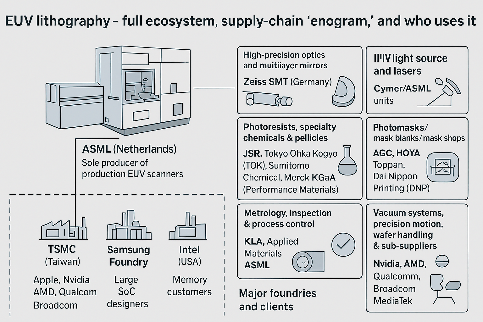
The EUV Supply Chain: A Global Web of Dependencies
The complexity of EUV machines necessitates a supply chain involving over 5,000 suppliers from around the world. No single nation possesses all the technologies, materials, and expertise required to build these systems independently.
Critical Component Suppliers
1. Light Source Technology
Cymer (San Diego, USA) – ASML subsidiary since 2013
- Develops and manufactures the laser-produced plasma light source
- The heart of the EUV system, generating 13.5nm wavelength light
- Employs CO2 laser technology striking molten tin droplets
- Investment: ASML acquired Cymer for $2.5 billion
Trumpf (Ditzingen, Germany)
- Supplies the high-power CO2 lasers used in the light source
- Produces lasers delivering up to 40 kilowatts of power
- Critical technology that took decades to develop
- Exclusive partnership with ASML for EUV applications
2. Optical Systems
Carl Zeiss SMT (Oberkochen, Germany) – 24.9% owned by ASML
- Manufactures the ultra-precise mirrors for EUV systems
- Each mirror has surface roughness of less than 0.1 nanometers
- Takes months to produce a single mirror set
- Only company in the world capable of producing these optics
- Employs ion beam figuring technology for mirror shaping
3. Mechanical and Precision Components
VDL Group (Netherlands)
- Supplies precision mechanical modules and frames
- Manufactures clean room equipment
- Provides complex mechanical assemblies
Prodrive Technologies (Netherlands)
- Electronic systems and motion control
- Power electronics for laser systems
- Embedded computing platforms
ASML Berlin (Germany)
- Wafer stage and reticle stage systems
- Ultra-precise positioning technology (accuracy to picometers)
- Magnetic levitation systems
4. Materials and Coatings
Entegris (USA)
- Advanced materials for wafer handling
- Contamination control solutions
- Critical fluid handling systems
Shin-Etsu Chemical (Japan)
- Photomask blanks
- High-purity silicon materials
- Synthetic quartz glass
JSR Corporation (Japan)
- EUV photoresists
- Advanced materials for semiconductor manufacturing
- Chemical formulations specific to EUV wavelengths
Tokyo Ohka Kogyo (TOK, Japan)
- EUV photoresists
- Ancillary chemicals for lithography processes
5. Vacuum and Environmental Control
Atlas Copco (Sweden)
- Vacuum pumps and systems
- The EUV process requires near-perfect vacuum conditions
- Handles hydrogen purge systems
Edwards Vacuum (UK)
- High-vacuum technology
- Contamination prevention systems
6. Metrology and Inspection
KLA Corporation (USA)
- Provides metrology equipment for mask and wafer inspection
- Partners with ASML for integrated solutions
- Critical for quality control in EUV processes
7. Power and Control Systems
Philips (Netherlands)
- Legacy partner providing various subsystems
- Power conversion systems
- Specialized electronics
Siemens (Germany)
- Industrial automation systems
- Control software and hardware
- Manufacturing execution systems
Supply Chain Vulnerabilities and Geopolitical Implications
The EUV supply chain’s global nature creates significant geopolitical complexity. Key dependencies include:
- US Technology: Light source lasers, software, metrology tools
- German Precision: Optics and mechanical systems
- Japanese Materials: Photoresists, chemicals, specialty materials
- Dutch Integration: Final assembly and system design
This interdependence has made EUV technology a focal point of international trade policy, particularly regarding exports to China. The United States, Netherlands, and Japan have coordinated export controls on advanced semiconductor manufacturing equipment, including EUV systems.
Major Chip Foundries Using EUV Technology
Taiwan Semiconductor Manufacturing Company (TSMC)
Overview: TSMC is the world’s largest dedicated semiconductor foundry and the biggest customer of ASML’s EUV systems. Founded in 1987 by Morris Chang, TSMC pioneered the pure-play foundry model, manufacturing chips designed by other companies rather than producing its own designs.
Headquarters: Hsinchu, Taiwan
Market Position:
- Controls approximately 60% of the global foundry market
- Revenue: Over $70 billion (2023)
- Employees: Over 75,000 worldwide
EUV Deployment: TSMC has been the most aggressive adopter of EUV technology:
- First to implement 7nm EUV process (N7+) in 2019
- Currently manufacturing at 3nm with extensive EUV usage
- Developing 2nm process with High-NA EUV capability
- Owns over 200 EUV machines, more than any other company
- Plans to acquire High-NA EUV systems for sub-2nm nodes
Global Manufacturing Facilities:
Taiwan Operations:
- Fab 12 (Hsinchu): 300mm, 16nm and above
- Fab 14 (Tainan): 300mm, 7nm and 5nm with EUV
- Fab 15 (Central Taiwan Science Park): 300mm, 28nm
- Fab 18 (Tainan): 300mm, 5nm and 3nm with extensive EUV, largest fab
- Fab 20 (Hsinchu): 300mm, under construction for 2nm process
International Subsidiaries and Facilities:
TSMC Arizona (United States):
- Location: Phoenix, Arizona
- Investment: $40 billion for two fabs
- First fab: 4nm process, production starting 2025
- Second fab: 3nm/2nm processes, planned for 2028
- Expected employment: 4,500 jobs
- Strategic importance: Addresses US semiconductor independence concerns
TSMC Japan:
- JASM (Japan Advanced Semiconductor Manufacturing): Kumamoto
- Joint venture with Sony and Denso
- Investment: $8.6 billion
- Process technology: 22nm and 28nm (mature nodes)
- Production started: Late 2024
- Second fab planned focusing on more advanced nodes
TSMC Nanjing (China):
- 16nm and 28nm production (no EUV)
- Operates under US export control restrictions
- Capacity: 20,000 wafers per month
TSMC Europe:
- Announced fab in Germany (Dresden region)
- Joint venture with Bosch, Infineon, and NXP
- Focus: Automotive and industrial chips
- Investment: €10 billion
- Expected operation: 2027
Major Clients:
Apple Inc. – Largest customer (~25% of revenue)
- A-series chips for iPhones (A16, A17 Pro)
- M-series chips for MacBooks and iPads (M3, M3 Pro, M3 Max, M3 Ultra)
- All produced on TSMC’s most advanced nodes (3nm and 5nm)
NVIDIA Corporation
- GPU chips for data centers (H100, H200)
- AI accelerators (A100)
- Gaming GPUs (RTX 40-series)
- Uses 5nm and 4nm processes
Advanced Micro Devices (AMD)
- Ryzen processors (7nm, 5nm)
- EPYC server processors
- Radeon graphics chips
- MI300 AI accelerators on 5nm
Qualcomm
- Snapdragon mobile processors
- 5G modem chips
- IoT and automotive solutions
- 4nm and 5nm processes
MediaTek
- Smartphone processors (Dimensity series)
- Smart TV chips
- IoT solutions
Broadcom
- Networking chips
- Custom AI accelerators for Google
- Infrastructure semiconductors
Intel Corporation (Emerging customer)
- Outsourcing some production for GPU tiles
- Future CPU components
- Part of Intel’s IDM 2.0 strategy
Amazon (AWS)
- Custom Graviton server processors
- AI training chips (Trainium)
- Inference processors (Inferentia)
Samsung Foundry
Overview: Samsung Foundry, the semiconductor manufacturing division of Samsung Electronics, is the world’s second-largest foundry and TSMC’s primary competitor. Unlike TSMC’s pure-play model, Samsung Foundry is part of an integrated device manufacturer (IDM) that also designs and sells its own chips.
Headquarters: Hwaseong and Pyeongtaek, South Korea
Market Position:
- Approximately 15-18% global foundry market share
- Revenue: $20+ billion in foundry business
- Part of Samsung Electronics’ Device Solutions Division
EUV Implementation: Samsung was actually the first to implement EUV in high-volume manufacturing:
- First 7nm EUV process launched in 2018
- Currently producing 3nm and 4nm chips with EUV
- Owns approximately 40-50 EUV machines
- Developing 2nm Gate-All-Around (GAA) transistor technology
- Committed to acquiring High-NA EUV systems
Manufacturing Facilities:
South Korea:
S3 Line (Hwaseong):
- Samsung’s primary advanced logic foundry
- 300mm wafer production
- 7nm, 5nm, 4nm, and 3nm with EUV
- Major expansion ongoing
Pyeongtaek Campus:
- P1: Memory-focused but includes foundry capacity
- P2: Under construction, will include advanced foundry lines
- P3: Planned for future expansion
- Total investment exceeding $200 billion over multiple phases
Giheung Facility:
- R&D and pilot production
- Process technology development
- 300mm lines for testing
International Plans:
Samsung Taylor (United States):
- Location: Taylor, Texas
- Investment: $17+ billion
- Planned production: 4nm and 3nm processes
- Expected operation: 2025-2026
- Will include EUV capability
- Strategic facility for US customers
Planned European Facility:
- Under consideration, no final location
- Focus on automotive and industrial applications
Major Clients:
Qualcomm
- Snapdragon 8 Gen 1 and Gen 2 (4nm)
- Second-source to TSMC for flagship processors
- Wireless communication chips
- Tensor G2 and G3 SoC for Pixel phones (5nm/4nm)
- Custom AI accelerators
- Future generation chips
NVIDIA
- Some GPU production (diversification strategy)
- Networking chips
AMD
- Some GPU components
- Exploring partnership for CPU production
Tesla
- Full Self-Driving (FSD) chips (earlier generations)
- Hardware 3.0 computer
Baidu
- AI chips for cloud computing
- Autonomous driving processors
Internal Samsung Products:
- Exynos mobile processors
- Image signal processors
- 5G modems
- IoT and automotive chips
Intel Foundry Services (IFS)
Overview: Intel Foundry Services, launched in 2021, represents Intel’s strategic pivot to become a major foundry player alongside its traditional IDM business. This marks a historic shift for Intel, which has traditionally manufactured only its own designs.
Headquarters: Santa Clara, California, USA
Market Position:
- Emerging player in foundry market (currently <5% share)
- Part of Intel’s “IDM 2.0” strategy
- Leveraging decades of manufacturing expertise
- Unique position as Western foundry with advanced technology
EUV Strategy: Intel has been developing EUV capability:
- Deployed EUV in its Intel 4 process (20A node equivalent)
- Intel 3 and Intel 18A nodes will use extensive EUV
- Owns approximately 15-20 EUV machines (growing)
- Committed to High-NA EUV acquisition for Intel 18A and beyond
- First to receive ASML’s High-NA EUV system (2024)
Global Manufacturing Network:
United States:
Fab 52/62 (Arizona):
- Ocotillo campus expansion
- Investment: $20+ billion
- Intel 4 and Intel 3 processes
- EUV-equipped facilities
- Target production: 2024-2025
Ohio Megafab:
- Location: New Albany, Ohio
- Investment: Up to $100 billion over decade
- Two fabs initially, expandable to eight
- Advanced packaging and foundry services
- Expected operation: 2025-2027
- Will include extensive EUV capability
New Mexico:
- Research and development
- Pilot production lines
- Advanced packaging development
Oregon (Hillsboro):
- D1X: Development fab for new processes
- Intel 4, Intel 3, Intel 20A testing
- Primary R&D location
International Facilities:
Ireland (Leixlip):
- Fab 34: Intel 4 production planned
- Continuous expansion
- €12 billion investment phase
- Will receive EUV systems
Israel (Kiryat Gat):
- Fab 28: Production facility
- $25 billion expansion announced
- Advanced process technology
Germany (Magdeburg):
- Planned mega-fab investment: €30 billion
- Two leading-edge fabs
- Expected operation: 2027-2029
- Strategic facility for European customers
Poland (Wrocław):
- Advanced packaging and test facility
- Investment: $4.6 billion
Malaysia:
- Advanced packaging and testing
- Long-standing operations
Major and Potential Clients:
Confirmed Clients:
Amazon (AWS)
- Custom server chips
- Long-term partnership announced
- Intel 18A process expected
US Department of Defense
- Secure Enclave program
- Trusted domestic semiconductor source
- Advanced military-grade chips
Ericsson
- 5G infrastructure chips
- Custom silicon for telecom
- Intel 18A process
MediaTek
- Partnership for advanced chip production
- Future product lines
Microsoft
- Potential custom chips for Azure cloud
- Gaming processors
- Under discussion for future projects
Potential Clients Being Courted:
- Qualcomm (diversification from TSMC/Samsung)
- NVIDIA (second-source strategy)
- AMD (tactical partnership despite competition)
- Various fabless semiconductor companies
GlobalFoundries
Overview: GlobalFoundries, formed from AMD’s manufacturing spin-off in 2009, is the world’s third-largest foundry. Importantly, GlobalFoundries does NOT use EUV technology—the company announced in 2018 it would cease development of 7nm and more advanced processes, focusing instead on mature and specialty process technologies.
Headquarters: Malta, New York, USA (owned by Mubadala Investment Company of UAE)
Market Position:
- Approximately 6-7% global foundry market share
- Revenue: ~$8 billion
- Focus: Mature nodes (12nm and above), specialty processes
- Leader in RF, automotive, and IoT chip manufacturing
Why Include GlobalFoundries? While GlobalFoundries doesn’t use EUV, it’s important to understand the complete foundry ecosystem. Many chips don’t require cutting-edge processes, and GlobalFoundries serves critical markets including:
- Automotive microcontrollers
- RF and wireless communication chips
- Power management ICs
- IoT sensors and controllers
- Display drivers
Global Manufacturing Facilities:
Fab 8 (Malta, New York, USA):
- 300mm wafer production
- 12nm, 14nm processes
- Automotive and RF focus
Fab 9 (Burlington, Vermont, USA):
- 200mm and 300mm
- Specialty technologies
- RF-SOI processes
Fab 1 (Dresden, Germany):
- 300mm production
- 22nm FD-SOI technology
- Automotive and industrial focus
Singapore:
- Fab 7: 300mm, 40nm and above
- Fab 3E: 200mm specialty processes
- Fab 2: 200mm production
Major Clients:
- Qualcomm (RF front-end chips)
- AMD (I/O dies for chiplet processors)
- NXP Semiconductors
- STMicroelectronics
- Broadcom
- Automotive manufacturers (through Tier 1 suppliers)
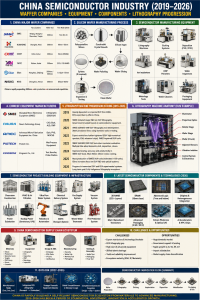
SMIC (Semiconductor Manufacturing International Corporation)
Overview: SMIC is China’s largest and most advanced semiconductor foundry, representing the nation’s ambitions to achieve semiconductor self-sufficiency. However, SMIC’s access to EUV technology is blocked by export controls imposed by the Netherlands, United States, and Japan.
Headquarters: Shanghai, China
Market Position:
- Largest foundry in China (~6% global market share)
- Revenue: ~$7 billion (2023)
- State-supported development
- Partial state ownership
EUV Status and Challenges: SMIC does NOT have access to EUV technology:
- Export controls prevent ASML from selling EUV systems to China
- Limited to DUV lithography equipment
- Achieved 7nm production using multi-patterning DUV techniques (controversial and unverified)
- Significantly disadvantaged versus TSMC and Samsung in advanced nodes
- Relying on older technology and innovative process techniques
Manufacturing Facilities:
China:
Shanghai:
- Multiple 300mm fabs
- 14nm, 28nm, 40nm processes
- Headquarters and primary operations
Beijing:
- 300mm production
- Joint venture structure
- Advanced process development
Tianjin:
- 200mm fab
- Mature process technologies
Shenzhen:
- 200mm and 300mm lines
- South China manufacturing hub
Major Clients:
- Qualcomm (mature node chips)
- Broadcom
- HiSilicon (Huawei’s chip design arm – limited by sanctions)
- Chinese smartphone makers (Xiaomi, Oppo, Vivo)
- Chinese fabless semiconductor companies
- Bitmain (cryptocurrency mining chips)
Geopolitical Context: SMIC represents the frontline of the US-China technology competition. The company has been:
- Added to US Entity List in 2020, restricting technology access
- Prevented from acquiring EUV systems
- Subject to restrictions on advanced DUV equipment
- Focus of Chinese government’s semiconductor independence efforts
Other Notable Foundries
United Microelectronics Corporation (UMC) – Taiwan
- Fourth-largest pure-play foundry globally
- No EUV technology
- Focus on mature and specialty processes (14nm and above)
- Clients: Qualcomm, MediaTek, Texas Instruments
Tower Semiconductor (Now Intel-owned) – Israel
- Specialty foundry acquired by Intel in 2023
- No EUV technology
- Focus on analog and mixed-signal processes
- Strengthens Intel Foundry Services portfolio
Hua Hong Semiconductor – China
- Second-largest Chinese foundry
- No EUV access
- Focus on power management, embedded memory
- Multiple fabs in Shanghai and Wuxi
The Client Ecosystem: Who Needs Advanced Chips?
Smartphone and Consumer Electronics Giants
Apple
- Largest consumer of cutting-edge EUV-manufactured chips
- Designs A-series and M-series processors in-house
- Exclusively uses TSMC for manufacturing
- Annual chip procurement: tens of billions of dollars
- Drives demand for 3nm technology
Samsung Electronics
- Both foundry operator and customer
- Uses internal foundry for Exynos chips
- Also uses TSMC and Samsung Foundry for various components
- Custom Tensor chips for Pixel phones (Samsung Foundry)
- TPU (Tensor Processing Unit) AI accelerators
- Growing in-house chip design capability
AI and Data Center Leaders
NVIDIA
- Dominant player in AI and GPU computing
- H100, A100 data center GPUs manufactured by TSMC
- Driving massive demand for advanced process nodes
- Critical customer for EUV-manufactured chips
AMD
- Ryzen, EPYC, Radeon, and MI300 series
- Relies entirely on external foundries (primarily TSMC)
- Competing with Intel and NVIDIA
Amazon Web Services (AWS)
- Custom Graviton processors
- AI training and inference chips
- Growing internal chip design team
Microsoft
- Azure Maia AI accelerator
- Custom silicon for data centers
- Strategic relationship with multiple foundries
Meta (Facebook)
- AI inference accelerators
- Video processing chips
- Data center optimization silicon
Google Cloud
- TPU chips for AI workloads
- Custom networking silicon
- Video transcoding accelerators
Automotive and Industrial
Tesla
- Full Self-Driving computer chips
- Custom AI accelerators for vehicles
- Manufactured at Samsung Foundry
Automotive Tier 1 Suppliers:
- Bosch
- Continental
- Denso
- Driving demand for automotive-grade chips at various nodes
Telecom and Networking
Qualcomm
- Snapdragon mobile processors
- 5G modems and RF front-end
- Major customer of TSMC and Samsung
MediaTek
- Smartphone processors
- TV and smart home chips
- Primarily TSMC customer
Broadcom
- Networking infrastructure
- Custom accelerators
- Multiple foundry relationships
Supply Chain Security and Future Outlook
Critical Vulnerabilities
The semiconductor supply chain faces several key vulnerabilities:
- Single-Source Dependency: Only ASML can make EUV machines
- Geographic Concentration: 90%+ of advanced chips made in Taiwan
- Geopolitical Tensions: Taiwan-China relations create supply risk
- Complex Dependencies: No single country can independently produce advanced chips
- Long Lead Times: New fabs take 3-5 years to build and cost $10-20 billion
Reshoring and Diversification Efforts
United States:
- CHIPS Act: $52 billion in subsidies
- TSMC Arizona, Intel Ohio, Samsung Texas facilities
- Goal: Produce 20% of world’s advanced chips domestically by 2030
Europe:
- European Chips Act: €43 billion in investment
- TSMC Germany, Intel Germany facilities planned
- Focus on achieving 20% global chip production share
Japan:
- Subsidizing TSMC fab in Kumamoto
- Revitalizing domestic semiconductor industry
- Partnership strategy with foreign foundries
China:
- “Big Fund” investments exceeding $100 billion
- Focus on self-sufficiency despite technology restrictions
- Alternative technology pathways being explored
Technology Roadmap
High-NA EUV:
- Next-generation EUV with 0.55 numerical aperture
- Enables sub-2nm manufacturing
- ASML shipping first systems in 2024-2025
- Intel first customer, TSMC and Samsung to follow
Chiplet and Advanced Packaging:
- Moving from 2D scaling to 3D integration
- TSMC’s 3D fabric, Intel’s Foveros
- Enables continued performance improvements beyond traditional scaling
Gate-All-Around (GAA) Transistors:
- Samsung’s 3nm and beyond
- TSMC’s future nodes
- Replacing FinFET architecture
Quantum and Photonics:
- Long-term alternatives to silicon CMOS
- Still in research phase
- Potential for specialized applications
Economic and Strategic Implications
The EUV supply chain and advanced semiconductor manufacturing represent perhaps the most strategically important technology ecosystem in the 21st century. The implications include:
Economic Impact:
- Semiconductor industry: $600+ billion annually
- Downstream impact: Trillions in electronics, AI, automotive, telecom
- Jobs: Millions directly and indirectly employed
- Innovation driver across all sectors
National Security:
- Military systems depend on advanced chips
- AI and quantum computing capabilities
- Communications and cyber security infrastructure
- Economic competitiveness as national security issue
Geopolitical Competition:
- US-China technology rivalry centered on semiconductors
- Taiwan’s critical importance to global economy
- European and Japanese strategic positioning
- Export controls as geopolitical tool
Environmental Considerations:
- Fab construction requires massive water and energy resources
- Single fab can use millions of gallons of ultrapure water daily
- Electricity consumption comparable to small cities
- Growing focus on sustainable semiconductor manufacturing
Conclusion
The EUV lithography supply chain represents one of the most complex technological and logistical achievements in human history. From the approximately 5,000 suppliers across dozens of countries contributing to each ASML machine, to the sophisticated foundries manufacturing billions of transistors on fingernail-sized chips, to the countless products and services that depend on these chips, the ecosystem is vast and deeply interconnected.
ASML’s monopoly on EUV technology, combined with the concentration of advanced manufacturing in Taiwan, creates both tremendous economic value and significant strategic vulnerability. The industry’s response—reshoring efforts in the US and Europe, technology diversification, and new manufacturing paradigms like chiplets—will shape the global economy and geopolitical landscape for decades to come.
As we move toward 2nm, 1.4nm, and eventually angstrom-scale manufacturing, the importance of EUV technology and the foundries that deploy it will only grow. The companies and countries that successfully navigate this complex supply chain will command the commanding heights of the 21st-century economy, while those left behind risk economic and strategic marginalization.

Be First to Comment