
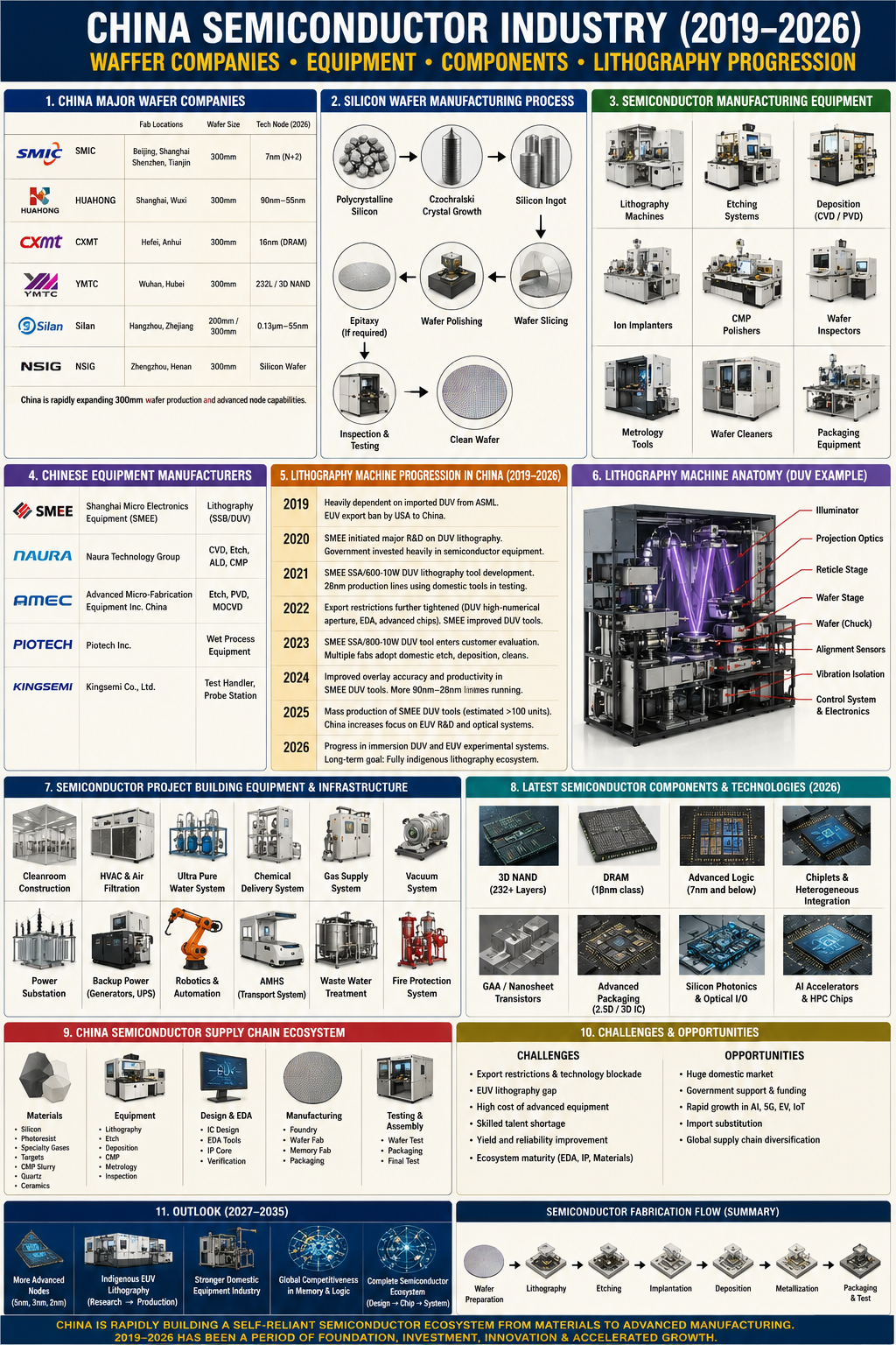
1. Introduction (Pages 1–2)
- Wafer‑fabrication companies and their strategic expansions
- Domestic and foreign semiconductor equipment ecosystems
- Latest components and process tools used in modern fabs
- Lithography machine development and constraints
- Policy, export‑control, and investment forces shaping the industry
- China’s localization roadmap and technological gaps
The period is defined by massive capital expenditure, AI‑driven demand, and geopolitical constraints that forced China to innovate under pressure.
2. China’s Wafer‑Fabrication Companies (Pages 3–8)
2.1 SMIC (Semiconductor Manufacturing International Corporation)
- Largest foundry in China
- Expanded 14 nm, 7 nm (restricted), and mature‑node production
- Dependent on foreign lithography tools (ASML DUV)
- Benefited from domestic etch, deposition, CMP tools
- Aggressive fab construction in Shanghai, Beijing, Shenzhen
2.2 YMTC (Yangtze Memory Technologies)
- China’s leading NAND flash manufacturer
- Phase‑2 fab expansion in 2024–2026
- Procurement pipeline for deposition, etch, CMP tools accelerated in 2026
- Export controls limited access to advanced deposition and metrology tools
2.3 CXMT (ChangXin Memory Technologies)
- China’s primary DRAM manufacturer
- 2026 tender for US$5–6 billion in equipment procurement
- Planned expansion: 50–60k wafers per year
- Major driver of domestic CMP, etch, and thin‑film equipment demand
2.4 Hua Hong Semiconductor
- Mature‑node specialist
- Focus on power devices, embedded memory
- Heavy user of domestic cleaning, etch, and packaging tools
2.5 Emerging Players (2023–2026)
- Nexchip
- Silan
- CR Micro
- Rapid adoption of domestic tools due to export restrictions
3. China’s Semiconductor Equipment Ecosystem (Pages 9–18)
China’s equipment ecosystem evolved from near‑zero global share in advanced tools to meaningful penetration in mid‑range segments.
3.1 Key Domestic Equipment Manufacturers
Etch Tools
- AMEC (Advanced Micro‑Fabrication Equipment)
- NAURA
- China gained 8 percentage‑point market share in dry etch tools from 2019–2024.
CMP Tools
- Hwatsing Technology
- Increased China’s CMP market share by eight percentage points.
Deposition Tools (PVD, CVD, ALD)
- NAURA, Piotech, AMEC
- Market share rose from 2% to 7% between 2019–2024.
Cleaning Tools
- Kingsemi
- Achieved 50–55% localization in single‑wafer cleaning by 2025.
Photoresist Stripping
- Domestic localization reached 65–70% by 2025.
Packaging & Test Tools
- Hangzhou Changchuan, AccoTEST
- China reached 70% market share in linear/discrete test tools.
4. Latest Components & Process Equipment (Pages 19–28)
4.1 Core Fab Equipment Categories
A modern fab requires hundreds of specialized tools:
- Lithography (EUV, DUV, i‑line)
- Etch (dry etch, plasma etch)
- Deposition (PVD, CVD, ALD)
- CMP (chemical mechanical planarization)
- Ion implantation
- Metrology & inspection
- Cleaning & photoresist stripping
- Coater‑developer systems
- Advanced packaging tools
China’s localization rates (2025 actuals):
- Etch: 30–35%
- CMP: 28–35%
- PVD: 20–25%
- PECVD: 18–22%
- ALD: 8–12%
- Coater‑developer: 10–12%
- Metrology: 12–15%
- Lithography: <5% (critical bottleneck)
4.2 Latest Components Introduced 2019–2026
- High‑uniformity plasma sources for etch
- Advanced ALD chambers for sub‑10 nm nodes
- Hybrid CMP pads and slurries
- High‑aspect‑ratio deposition reactors
- AI‑driven metrology systems
- Multi‑beam inspection tools
- High‑precision wafer‑handling robotics
4.3 Equipment Demand Drivers
- AI computing → HBM, DRAM, NAND demand
- EV industry → power semiconductors
- IoT → mature‑node expansion
- Export controls → domestic substitution
5. Lithography Machine Progression (Pages 29–38)
5.1 Global Lithography Landscape
- ASML (Netherlands): EUV & advanced DUV
- Nikon (Japan): DUV
- Canon (Japan): legacy nodes
- TEL (Japan): coater‑developer systems
These companies maintain 75–80% of global control over critical lithography‑related steps.
5.2 China’s Lithography Efforts (SMEE)
- Shanghai Micro Electronics Equipment (SMEE)
- Achieved 4% market share in i‑line lithography (legacy nodes)
- No domestic DUV immersion or EUV capability as of 2026
5.3 2019–2021: Foundation Stage
- SMEE delivered 90 nm–110 nm i‑line tools
- Heavy reliance on imported optics and subsystems
- ASML continued shipping DUV to China
5.4 2022–2024: Export‑Control Shock
- U.S. EAR tightened in 2022
- Netherlands restricted ASML DUV exports in 2024
- China accelerated domestic R&D
5.5 2025–2026: Localization Push
- Big Fund III launched in 2024 with RMB 344 billion (~$47 billion)
- Focus on lithography, materials, EDA, advanced nodes
- SMEE prototypes for 28 nm DUV (non‑immersion) under development
5.6 Remaining Bottlenecks
- Light sources (ArF immersion lasers)
- High‑precision optics
- Photoresist materials
- Stage control systems
- EUV mirrors (Zeiss monopoly)
6. Policy, Investment & Export Controls (Pages 39–44)
6.1 Government Investment
- Big Fund I (2014), Big Fund II (2019), Big Fund III (2024)
- 2024 fund: RMB 344 billion targeting equipment localization
6.2 Export Controls
- U.S. restrictions on sub‑14 nm equipment
- Netherlands restrictions on ASML DUV
- Japan restrictions on etch and deposition subsystems
- Result: forced domestic substitution and co‑development with Chinese fabs
6.3 Industrial Strategy
- “Made in China 2025”
- Localization staircase model
- Focus on mid‑range tools first, advanced tools later
7. Market Scale & Competitive Landscape (Pages 45–47)
7.1 Market Size
- China became the largest wafer‑fab expansion market globally
- Equipment market:
- $40 billion in 2024
- $49.3 billion in 2025 (+23%)
7.2 Competitive Dynamics
- Domestic firms rising in CMP, etch, deposition
- Foreign firms dominate lithography, metrology, ALD
- China’s share in advanced packaging tools increasing
8. 2019–2026 Timeline Summary (Page 48)
2019–2020
- Early domestic breakthroughs in CMP, cleaning
- SMEE i‑line tools mature
2021–2022
- Export controls intensify
- China accelerates etch/deposition R&D
2023–2024
- Major fab expansions (YMTC, CXMT)
- Netherlands restricts ASML DUV exports
- Big Fund III launched
2025–2026
- China reaches 43% of global equipment demand
- Domestic substitution accelerates
- Lithography remains <5% localized
9. Conclusion (Page 49)
Between 2019 and 2026, China’s semiconductor industry evolved into a global powerhouse in wafer‑fab expansion and mid‑range equipment localization. Domestic firms achieved significant gains in etch, deposition, CMP, cleaning, and packaging tools, driven by massive investments and geopolitical constraints. However, lithography—especially EUV and advanced DUV—remains the defining technological bottleneck. China’s future competitiveness hinges on breakthroughs in optics, lasers, materials, and precision engineering.
The 2019–2026 period represents both extraordinary progress and clear structural limits, shaping China’s semiconductor trajectory for the next decade.






Be First to Comment