
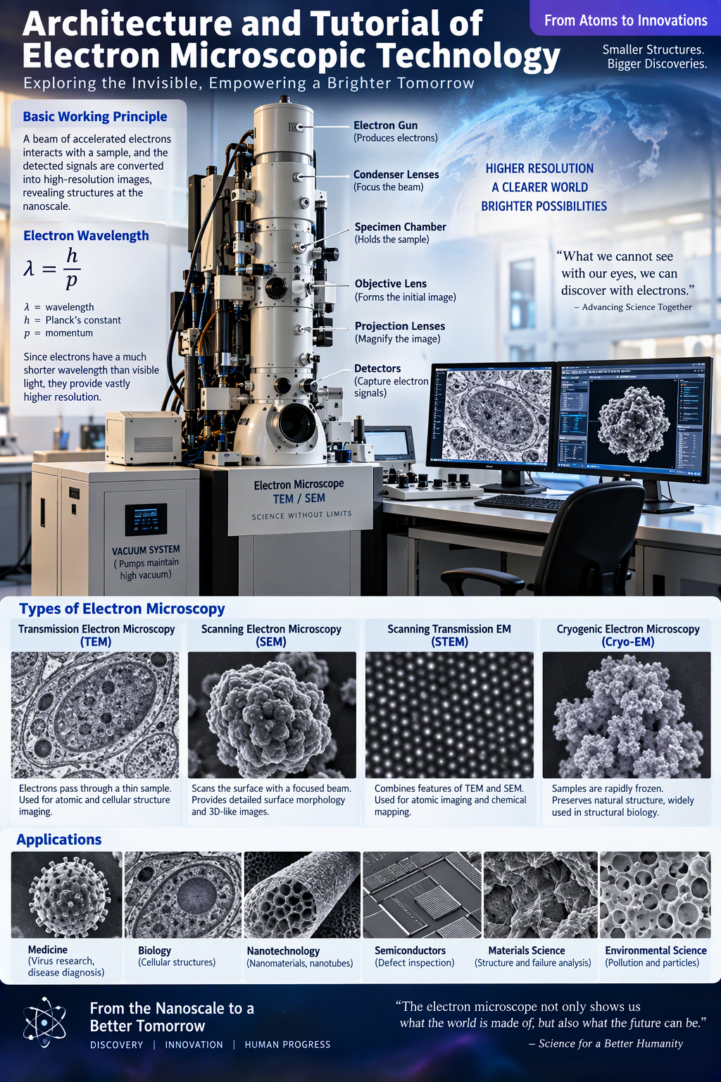
Title Page
Architecture and Tutorial of Electron Microscopic Technology: Principles, Design, Applications, and Future Innovations
Abstract
Electron microscopic technology represents one of humanity’s greatest scientific achievements in visualizing structures beyond the limitations of optical microscopy. By utilizing highly accelerated electrons instead of visible light, electron microscopes achieve resolutions thousands of times greater than conventional microscopes, allowing scientists to observe viruses, cellular organelles, nanomaterials, atomic structures, and molecular interactions.
This thesis provides a comprehensive exploration of electron microscopy, including its historical development, architecture, operational principles, instrumentation, applications, advantages, challenges, and future prospects. Particular attention is paid to the architecture of Transmission Electron Microscopy (TEM), Scanning Electron Microscopy (SEM), and emerging electron imaging systems that continue to transform medicine, biology, materials science, nanotechnology, aerospace engineering, and industrial quality control.
Table of Contents
Chapter 1: Introduction to Electron Microscopy
Chapter 2: Historical Development
Chapter 3: Fundamentals of Electron Theory
Chapter 4: Principles of Electron Beam Generation
Chapter 5: Architecture of Electron Microscopes
Chapter 6: Electron Sources and Guns
Chapter 7: Electromagnetic Lens Systems
Chapter 8: Vacuum Technology
Chapter 9: Transmission Electron Microscopy (TEM)
Chapter 10: Scanning Electron Microscopy (SEM)
Chapter 11: Scanning Transmission Electron Microscopy (STEM)
Chapter 12: Cryogenic Electron Microscopy
Chapter 13: Sample Preparation Techniques
Chapter 14: Image Formation Principles
Chapter 15: Resolution and Magnification
Chapter 16: Detection Systems
Chapter 17: Image Processing Technologies
Chapter 18: Biological Applications
Chapter 19: Medical Applications
Chapter 20: Nanotechnology Applications
Chapter 21: Industrial Applications
Chapter 22: Aerospace Applications
Chapter 23: Semiconductor Inspection
Chapter 24: Materials Science Research
Chapter 25: Failure Analysis
Chapter 26: Forensic Science Uses
Chapter 27: Environmental Applications
Chapter 28: Data Analysis and AI Integration
Chapter 29: Safety Protocols
Chapter 30: Maintenance Procedures
Chapter 31: Comparative Analysis with Optical Microscopy
Chapter 32: Limitations and Challenges
Chapter 33: Emerging Technologies
Chapter 34: Quantum Electron Imaging
Chapter 35: Future Innovations
Chapter 36: Economic Impact
Chapter 37: Educational Importance
Chapter 38: Global Scientific Contributions
Chapter 39: Advanced Electron Detectors
Chapter 40: Atomic Scale Imaging
Chapter 41: Three-Dimensional Electron Microscopy
Chapter 42: Artificial Intelligence Enhancement
Chapter 43: Future Medical Diagnostics
Chapter 44: Vision of Next-Generation Electron Microscopes
Chapter 45: Conclusion
Chapter 1: Introduction to Electron Microscopy
Electron microscopy is a scientific imaging technology that uses streams of accelerated electrons to visualize objects too small to be observed with traditional light microscopes. Since electrons possess wavelengths much shorter than visible light, they enable observation at nanometer and even atomic scales.
The technology has revolutionized scientific understanding by revealing intracellular structures, viruses, crystal lattices, proteins, and nanoscale materials.
Chapter 2: Historical Development
The conceptual foundation of electron microscopy emerged from Louis de Broglie’s wave-particle theory proposed in 1924. Ernst Ruska and Max Knoll successfully built the first electron microscope in 1931.
Major milestones include:
- First TEM development
- Commercial SEM systems
- Cryo-electron microscopy invention
- Digital imaging integration
- AI-assisted microscopy
Ruska later received the Nobel Prize for his pioneering contributions.
Chapter 3: Fundamentals of Electron Theory
Electrons possess:
- Mass
- Charge
- Momentum
- Wave properties
According to quantum mechanics:
λ = h/p
where:
- λ = wavelength
- h = Planck’s constant
- p = momentum
The shorter wavelength provides electron microscopes with vastly superior resolution.
Chapter 4: Principles of Electron Beam Generation
Electron beams are generated through:
- Thermionic Emission
- Field Emission
- Schottky Emission
The beam is accelerated using high-voltage systems ranging from:
- 1 kV
- 30 kV
- 100 kV
- 300 kV
- Above 1000 kV
These energies determine penetration power and resolution.
Chapter 5: Architecture of Electron Microscopes
The architecture contains:
Electron Source
Produces electrons.
Condenser Lens
Focuses beam.
Specimen Chamber
Contains sample.
Objective Lens
Creates initial image.
Projection Lens
Magnifies image.
Detector System
Captures electron information.
Computer Interface
Processes images.
Overall architecture resembles a highly integrated nanoscopic imaging factory.
Chapter 6: Electron Sources and Guns
Electron guns serve as the heart of microscope operation.
Main types:
Tungsten Filament Gun
Advantages:
- Simple
- Affordable
LaB6 Gun
Advantages:
- Higher brightness
- Better stability
Field Emission Gun
Advantages:
- Highest resolution
- Narrow beam diameter
Chapter 7: Electromagnetic Lens Systems
Unlike optical microscopes using glass lenses, electron microscopes employ electromagnetic lenses.
Functions:
- Beam focusing
- Image magnification
- Aberration correction
Magnetic fields control electron trajectories with remarkable precision.
Chapter 8: Vacuum Technology
Electrons collide easily with gas molecules.
Therefore microscopes maintain:
- High Vacuum
- Ultra-High Vacuum
Vacuum pumps include:
- Rotary pumps
- Diffusion pumps
- Turbomolecular pumps
- Ion pumps
Chapter 9: Transmission Electron Microscopy (TEM)
TEM transmits electrons through extremely thin specimens.
Capabilities:
- Cellular ultrastructure observation
- Viral imaging
- Crystal analysis
- Protein visualization
Resolution reaches below 0.1 nanometers.
Chapter 10: Scanning Electron Microscopy (SEM)
SEM scans surfaces using focused electron beams.
Advantages:
- Large depth of field
- Surface morphology visualization
- 3D-like appearance
Applications include metallurgy, electronics, and biology.
Chapter 11: Scanning Transmission Electron Microscopy (STEM)
STEM combines characteristics of TEM and SEM.
Benefits:
- Atomic imaging
- Chemical mapping
- Materials characterization
Widely used in nanotechnology.
Chapter 12: Cryogenic Electron Microscopy
Cryo-EM freezes biological specimens rapidly.
Benefits include:
- Preserving natural structure
- Eliminating chemical fixation
- High molecular resolution
Cryo-EM has transformed structural biology.
Chapter 13: Sample Preparation Techniques
Preparation methods include:
- Fixation
- Dehydration
- Embedding
- Sectioning
- Coating
- Freezing
Proper preparation directly determines image quality.
Chapter 14: Image Formation Principles
Image formation involves:
- Electron emission
- Beam focusing
- Sample interaction
- Signal generation
- Detection
- Image reconstruction
Each stage influences final resolution.
Chapter 15: Resolution and Magnification
Electron microscopes achieve:
| Technology | Resolution |
|---|---|
| Light Microscope | 200 nm |
| SEM | 1-10 nm |
| TEM | <0.1 nm |
This makes atomic imaging possible.
Chapter 16: Detection Systems
Common detectors include:
- Secondary Electron Detectors
- Backscattered Electron Detectors
- CCD Cameras
- CMOS Sensors
- Hybrid Pixel Detectors
Chapter 17: Image Processing Technologies
Modern software performs:
- Noise reduction
- Contrast enhancement
- Pattern recognition
- Automated measurements
- AI-assisted reconstruction
Chapter 18: Biological Applications
Electron microscopes reveal:
- Mitochondria
- Ribosomes
- Membranes
- DNA interactions
- Cellular organelles
They expanded modern biology tremendously.
Chapter 19: Medical Applications
Medical researchers use electron microscopy to study:
- Viruses
- Cancer cells
- Protein complexes
- Infectious diseases
- Neurodegenerative disorders
Chapter 20: Nanotechnology Applications
Nanotechnology depends heavily upon electron microscopes.
Scientists visualize:
- Nanotubes
- Nanoparticles
- Nanowires
- Nanocomposites
Chapter 21–30: Industrial and Operational Applications
Applications include:
Semiconductor Manufacturing
Defect inspection.
Aerospace Engineering
Material testing.
Automotive Industry
Failure analysis.
Energy Systems
Battery characterization.
Environmental Science
Pollution monitoring.
Forensics
Evidence examination.
Quality Control
Microscopic defect detection.
Safety and Maintenance
Equipment preservation.
Data Management
Digital archiving.
Research Optimization
Scientific productivity enhancement.
Chapter 31: Comparison with Optical Microscopy
Electron microscopes outperform optical systems in:
- Resolution
- Magnification
- Atomic observation
However optical microscopes remain cheaper and easier to operate.
Chapter 32: Limitations and Challenges
Major challenges include:
- High cost
- Complex operation
- Vacuum requirements
- Radiation damage
- Extensive training needs
Chapter 33: Emerging Technologies
Current innovations:
- Aberration correction
- Ultrafast microscopy
- Quantum detectors
- AI-assisted imaging
Chapter 34: Quantum Electron Imaging
Future systems exploit:
- Quantum coherence
- Wave interference
- Atomic-scale precision
These techniques promise unprecedented imaging capabilities.
Chapter 35: Future Innovations
Expected advancements include:
- Portable electron microscopes
- Automated laboratories
- Remote operation
- Robotic sample handling
- Real-time molecular tracking
Chapter 36: Economic Impact
Electron microscopy supports industries worth trillions worldwide through:
- Manufacturing
- Pharmaceuticals
- Nanotechnology
- Electronics
- Biomedical research
Chapter 37: Educational Importance
Universities employ electron microscopy to teach:
- Cell biology
- Materials science
- Physics
- Engineering
Chapter 38: Global Scientific Contributions
Electron microscopes have enabled discoveries involving:
- DNA organization
- Protein structures
- Virus identification
- Advanced materials
Chapter 39: Advanced Electron Detectors
Next-generation detectors provide:
- Higher sensitivity
- Faster acquisition
- Lower noise
- Better accuracy
Chapter 40: Atomic Scale Imaging
Modern TEM systems routinely image:
- Individual atoms
- Crystal defects
- Atomic bonds
This capability drives nanotechnology development.
Chapter 41: Three-Dimensional Electron Microscopy
3D reconstruction techniques create:
- Cellular models
- Molecular maps
- Industrial surface structures
Chapter 42: Artificial Intelligence Enhancement
AI now performs:
- Automated focusing
- Defect recognition
- Pattern analysis
- Image segmentation
The combination of AI and microscopy is transforming research productivity.
Chapter 43: Future Medical Diagnostics
Future applications may include:
- Personalized diagnostics
- Early disease detection
- Cancer screening
- Precision medicine
Chapter 44: Vision of Next-Generation Electron Microscopes
Future systems may possess:
- Atomic tomography
- Quantum-enhanced detectors
- Autonomous operation
- Cloud integration
- AI decision-making systems
Chapter 45: Conclusion
Electron microscopic technology stands among humanity’s most powerful scientific inventions. Through sophisticated integration of quantum physics, electromagnetic engineering, computational science, vacuum technology, and advanced imaging systems, electron microscopes have opened a window into the nanoscale world.
Their architecture enables scientists to visualize structures from viruses to individual atoms, dramatically advancing biology, medicine, materials science, nanotechnology, aerospace engineering, and industrial manufacturing. As artificial intelligence, quantum technologies, and automation continue evolving, future electron microscopes will provide even greater resolution, speed, and analytical capabilities.
The continued development of electron microscopic technology will remain essential to scientific discovery, economic development, healthcare innovation, and humanity’s pursuit of understanding the microscopic foundations of life and matter.






Be First to Comment