
Introduction
The semiconductor industry has undergone a remarkable transformation over the past decade, with transistor technologies shrinking from 28 nanometers to just 3 nanometers. This journey represents not merely a linear reduction in size, but rather a series of revolutionary innovations that have fundamentally changed how engineers design and fabricate integrated circuits. As Moore’s Law continues to guide the industry forward, manufacturers have overcome increasingly complex physical challenges to pack ever more transistors into smaller spaces while maintaining or improving performance and power efficiency.
This article explores the major transistor technologies that have enabled this miniaturization, examining the innovations, challenges, and breakthroughs that characterize each generation. From the planar transistors of the 28nm era to the gate-all-around (GAA) structures of today’s cutting edge, we will trace the evolution of transistor design and understand how each technological leap has pushed the boundaries of what’s possible in chip design.
The 28nm Node: Traditional Planar Transistors
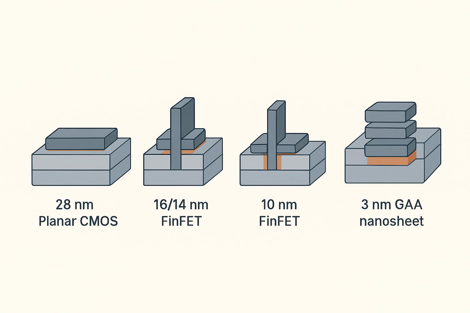
The 28-nanometer node, which became widespread around 2011, represents the transition point where traditional planar transistor scaling began to show signs of strain. At this node, manufacturers were still using relatively conventional planar metal-oxide-semiconductor field-effect transistors (MOSFETs), where the gate electrode sits on top of the silicon channel.
At 28nm, the critical challenge was leakage current. As transistors became smaller, the gate oxide layers grew thinner, and quantum tunneling effects became more pronounced, allowing electrons to leak through the oxide even when transistors were supposedly turned off. This leakage consumed power without performing any useful computation, reducing battery life in mobile devices and increasing cooling requirements in data centers.
To combat leakage, manufacturers introduced high-k dielectric materials and metal gates. Traditional silicon dioxide (SiO2) with a polysilicon gate gave way to hafnium-based dielectrics with work-function-tuned metal gates, typically using titanium nitride or other transition metal compounds. These materials allowed for thicker oxide layers without sacrificing capacitance, reducing leakage significantly while maintaining switching speed.
The 28nm node also saw the introduction of strain engineering to boost transistor performance. By creating controlled mechanical stress in the silicon channel, engineers could increase the mobility of charge carriers, allowing faster electron or hole transport and thus higher transistor speeds with lower supply voltages.
The 22nm and 20nm Nodes: Early FinFET Introduction
The move to 22 nanometers marked a pivotal transition in transistor design. Intel led the charge with their 22nm process, which introduced the FinFET (Fin Field-Effect Transistor) architecture. Rather than having the gate contact only the top surface of the silicon channel, the FinFET wraps the gate around a thin vertical fin of silicon, creating a three-sided gate contact.
This three-dimensional structure provided several profound advantages. The most significant was dramatically improved gate control. By wrapping the gate around the fin, manufacturers could suppress short-channel effects—parasitic phenomena where the channel becomes harder to control as transistors shrink. The increased gate surface area meant the gate could more effectively turn the transistor on and off, reducing subthreshold swing and leakage current.
The FinFET architecture also increased current density per unit area because the device could be made taller rather than wider, effectively increasing the channel width without increasing the transistor’s footprint. This meant smaller die sizes for the same number of transistors, or more transistors on the same die.
Samsung and Taiwan Semiconductor Manufacturing Company (TSMC) followed with their own 20nm and 14nm FinFET processes, each iteration refining the fin geometry and oxide materials. The fin width, typically 5-10 nanometers, became as important a parameter as the gate length in determining transistor performance.
FinFETs dominated chip design from roughly 2012 through 2020, with continuous iterations at 14nm, 10nm, 7nm, and 5nm nodes. Each generation improved fin geometry, reduced defects, and enhanced performance and power efficiency.
The 14nm Node: FinFET Maturity
By 14 nanometers, FinFET technology had matured considerably. Manufacturers had refined the process to achieve high yields while packing significantly more transistors per square millimeter. The 14nm node became particularly popular in mobile processors and data center CPUs because it offered an excellent balance between performance, power consumption, and cost.
One key development at 14nm was the introduction of multiple transistor flavors on the same die. Designers could specify different fin dimensions and oxide thicknesses for different regions of the chip, creating high-performance transistors with low leakage in critical paths, while using smaller, more leaky but faster transistors in less timing-sensitive areas. This heterogeneous transistor approach improved overall chip efficiency.
Strain engineering also advanced further, with manufacturers implementing both uniaxial and biaxial strain through carefully engineered layers beneath the transistor channel. By 14nm, the process matured to the point where companies like Apple, Qualcomm, and AMD could design leading-edge smartphones and computing devices.
The 10nm Node: Pushing FinFET Limits
The transition to 10 nanometers represented a more difficult jump than previous generations. The physical limits of FinFET architecture were becoming apparent. At 10nm, fin dimensions—already just 5-6 nanometers wide—were approaching the atomic scale. Quantum mechanical effects became increasingly problematic, and maintaining fin uniformity across an entire wafer became exponentially more challenging.
At 10nm, manufacturers continued to refine FinFET, introducing even more aggressive strain and beginning to experiment with alternative geometries. Gate length scaling also continued, with effective gate lengths dropping to around 20-22 nanometers in many designs.
Another significant innovation at 10nm was the introduction of ultra-low-k dielectrics in interconnect layers to reduce parasitic capacitance in the wiring that connects transistors. As gate pitch (the distance between adjacent transistor gates) continued to shrink, the relative impact of interconnect delay and power consumption grew, making these innovations essential.
The 10nm node pushed FinFET to approximately its limit, and by the end of this generation, semiconductor companies were actively developing the next major architectural shift.
The 7nm Node: Extreme Ultraviolet and Peak FinFET
The 7-nanometer node represented FinFET at its practical limit and marked the introduction of extreme ultraviolet (EUV) lithography. Traditional deep ultraviolet (DUV) lithography had been used with increasingly complex multiple-patterning schemes to achieve the feature sizes required. EUV, with its much shorter wavelength of 13.5 nanometers, allowed direct printing of smaller features without these complex multi-patterning steps.
The introduction of EUV fundamentally changed chip manufacturing. Where 22nm-to-10nm processes required increasingly baroque schemes—such as self-aligned multiple patterning (SAMP) and quadruple patterning—EUV simplified the process. This improved yields, reduced defects, and made designs more manufacturable.
At 7nm, FinFET reached its peak performance. Fin dimensions had shrunk to around 5 nanometers in width, with fin pitch around 20-26 nanometers. Despite the extreme density, manufacturers achieved good control and reasonable leakage characteristics. The 7nm node was widely adopted by high-end processors from Apple, AMD, NVIDIA, and others, driving major advances in smartphone and computing performance.
However, even at 7nm, it was becoming clear that FinFET had approached fundamental scaling limits. Fins were so narrow that quantum confinement effects significantly modified their electronic properties. Statistical variations in fin width led to unacceptable variability in transistor performance. The industry recognized that a new architecture would be necessary for the next generation.
The 5nm Node: Early FinFET-Based and Pre-GAA
The transition to 5 nanometers initially still relied on heavily-optimized FinFET, but this node marked the beginning of the shift toward new architectures. TSMC and Samsung began early production of true 5nm nodes around 2020-2021, while Intel delayed their corresponding process node.
At the 5nm node, FinFET remained but with several modifications. Fin width had shrunk to approximately 4 nanometers, approaching the practical limit where quantum effects make the fin properties fundamentally different from bulk silicon. Oxide thickness continued to shrink, now measured in atomic layers of only a few atoms thick.
More importantly, at 5nm, some manufacturers began introducing complementary transistor designs on the same die to optimize for different device requirements. A significant innovation was the introduction of advanced lithography techniques like multiple patterning with EUV to achieve even smaller gate pitches and transistor spacings.
Some process nodes at the 5nm generation showed early signs of the architectural transition to come. Researchers at leading foundries began developing gate-all-around (GAA) transistor concepts, investigating how to extend the fin structure into a more sophisticated configuration that would continue Moore’s Law.
The 3nm Node: Gate-All-Around Revolution
The 3-nanometer node represents a fundamental inflection point in transistor technology—the introduction of gate-all-around (GAA) structures as the dominant architecture. After nearly a decade of FinFET dominance, the industry has transitioned to a new paradigm that promises to continue scaling for several more generations.
In a GAA transistor, rather than a three-sided gate (as in FinFET), the gate completely surrounds the channel from all four sides. This is achieved through a sophisticated stacking of nanowire transistors or by creating a structure where horizontal channels are surrounded by a gate electrode.
The GAA Architecture
The most common implementation of 3nm GAA uses nanowires or nanosheets. In the nanosheet approach, instead of a single narrow fin, the channel consists of multiple extremely thin sheets of silicon (typically 5-10 nanometers wide and 1-2 nanometers thick) stacked vertically. A single gate electrode surrounds all these sheets at once. This configuration provides several advantages over FinFET.
First, the complete gate wrapping provides superior gate control, allowing the gate to more effectively modulate current through the entire thickness of the channel. This reduces subthreshold swing and leakage current even further than FinFET.
Second, the stacked sheet geometry allows for a more efficient layout. Rather than being limited by fin width, designers can control the channel cross-section by adjusting the number and thickness of stacked sheets. This provides greater design flexibility and allows further optimization for performance versus power consumption.
Third, the GAA structure is inherently scalable. The gate length can continue to shrink, the number of sheets can be increased, and the sheet thickness and width can be adjusted—all independent parameters offering design flexibility.
3nm Implementation and Manufacturing
TSMC began mass production of their 3nm process (N3) in 2022, with Samsung following with their 3nm GAE (Gate-All-Around) process in 2023. Intel’s corresponding 20A and 18A processes use a variant called “Intel 4” with their own GAA implementation called “RibbonFETs.”
Manufacturing 3nm GAA transistors requires extreme precision. The nanosheets must be fabricated to within a few atomic layers of their target thickness. Process variation in sheet thickness, width, or stacking uniformity can significantly impact device performance and leakage.
The 3nm node also required continued innovation in lithography. EUV became essential at this node, used for the most critical features. High-NA (numerical aperture) EUV systems began deployment, offering even tighter focal margins and smaller feature sizes.
Performance and Power Characteristics
The 3nm node delivered significant improvements over 5nm. Transistor density increased by approximately 60-70% compared to 5nm, driven both by the improved gate control of GAA and by continued reduction in metal pitch (the spacing between metal lines). Gate length was further reduced to approximately 12-14 nanometers in many designs.
Power consumption per transistor improved through both reduced leakage (via better gate control) and reduced dynamic switching energy (through lower required supply voltages). Clock speeds modestly increased or remained comparable to 5nm, with the power savings being the primary benefit—critical for mobile and battery-powered devices.
The 3nm node represents a substantially different design paradigm from FinFET. It requires redesign of circuits and design methodology to exploit the improved gate control and stacking possibilities. Leading companies like Apple, NVIDIA, AMD, and others have released 3nm-based designs starting in 2023.
Beyond 3nm: Future Directions
While 3nm is the current state-of-the-art for mass production, the industry is already developing the next generation. Several promising directions are being explored:
Complementary FET (CFET) structures promise to stack P-type and N-type transistors directly on top of each other rather than side-by-side, potentially halving the area required for a standard logic gate. This technology is likely to be introduced around the 2nm node.
Further refinement of GAA with increasingly sophisticated stacking and gate length reduction represents the most likely near-term path. Some foundries have announced processes at 2nm and beyond that continue the GAA approach with continued incremental improvements.
Backside power delivery, where power and ground lines are routed on the underside of the transistor stack rather than winding between transistors, promises significant improvements in efficiency and reduced parasitic effects.
Alternative channel materials beyond silicon are also being researched. Germanium, III-V semiconductors, and other materials can offer improved carrier mobility for both N and P-type transistors, potentially allowing continued performance scaling beyond the limits of silicon alone.
Conclusion
The journey from 28 nanometers to 3 nanometers represents one of the most impressive sustained engineering achievements in human history. What appeared in 2011 to be approaching a hard physical limit has been overcome through successive waves of innovation: high-k/metal gate, strain engineering, FinFET, EUV lithography, and now gate-all-around transistors.
Each transition required not just incremental improvement but fundamental rethinking of transistor architecture and manufacturing process. What’s remarkable is that despite being told multiple times that scaling was reaching its limit, the industry has found creative solutions that continue to deliver improved performance, reduced power consumption, and lower costs per transistor.
The 3nm generation represents perhaps the most significant architectural shift since FinFET, transitioning to a fully three-dimensional structure that promises to continue Moore’s Law for at least another half-decade. As we look beyond 3nm, entirely new innovations—stacked transistors, alternative materials, and novel device architectures—suggest that the story of semiconductor scaling is far from over. The next chapter promises to be equally revolutionary.






Be First to Comment