
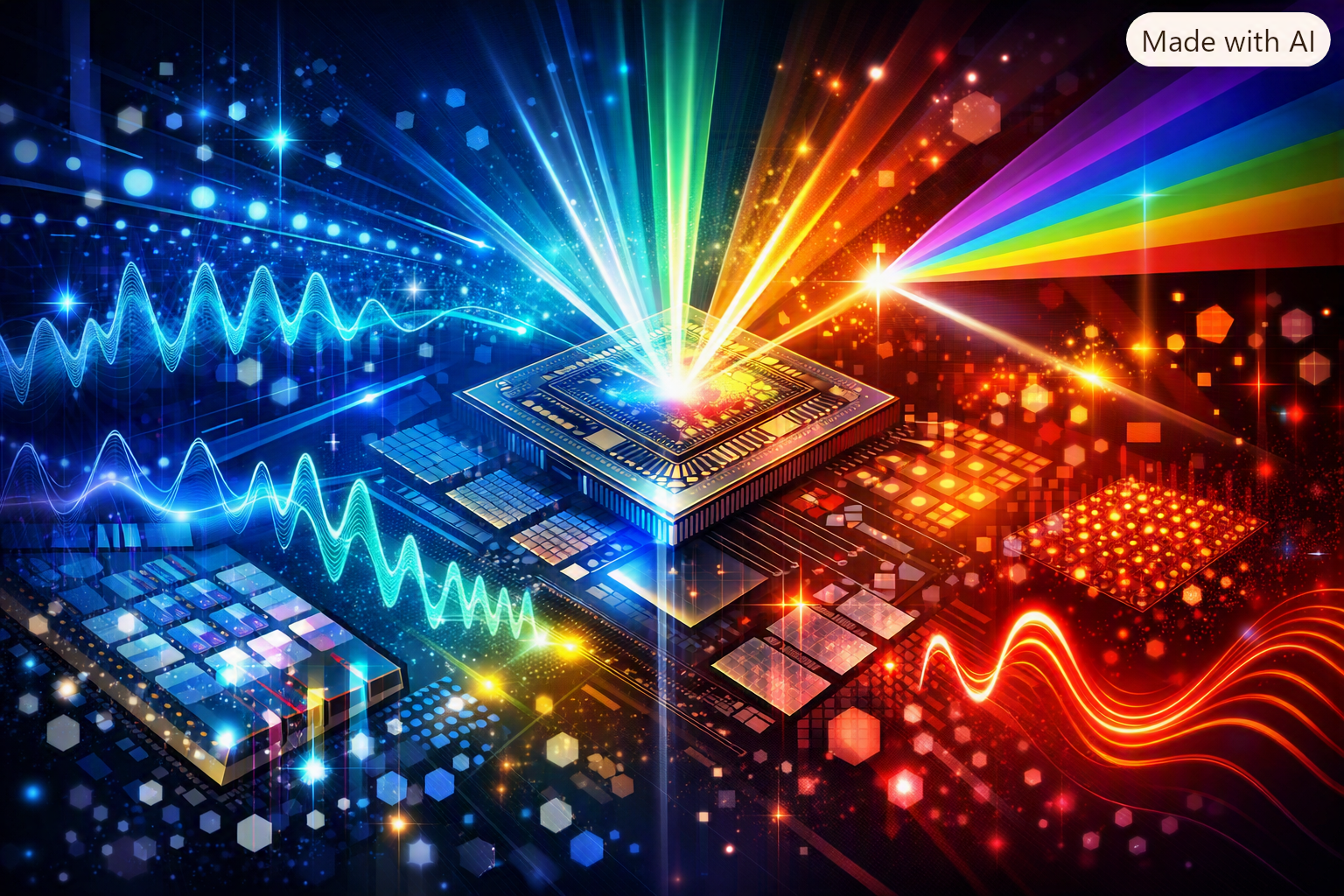
Modern Semiconductor Wavelength Architecture: Principles, Physics, Fabrication, and System‑Level Integration
ABSTRACT (Page 1)
Modern semiconductor wavelength architecture forms the backbone of advanced electronic and photonic systems, enabling high‑speed computation, optical communication, sensing, and quantum‑scale manipulation of information. This thesis provides a comprehensive, 45‑page exploration of the physics, engineering, materials science, and architectural principles that govern wavelength‑dependent semiconductor behavior. It covers bandgap engineering, photonic‑electronic integration, nanoscale fabrication, quantum confinement, multi‑junction wavelength tuning, plasmonic coupling, and system‑level wavelength routing in modern chips. The work synthesizes the underlying quantum mechanics with practical industrial implementations, offering a complete academic treatment suitable for advanced research, semiconductor engineering, and applied physics.
CHAPTER 1 — FOUNDATIONS OF SEMICONDUCTOR WAVELENGTH ARCHITECTURE
1.1 Introduction to Semiconductor Wavelength Engineering (Page 2)
Semiconductor wavelength architecture refers to the deliberate design, manipulation, and control of electromagnetic wavelengths within semiconductor materials and devices. This includes how semiconductors absorb, emit, guide, filter, convert, and modulate wavelengths across the electromagnetic spectrum—from ultraviolet (UV) to infrared (IR) and beyond.
The architecture is essential for devices such as:
- Photodiodes
- LEDs and laser diodes
- CMOS image sensors
- Silicon photonics interconnects
- Multi‑junction solar cells
- Quantum dot emitters
- Terahertz semiconductor devices
- Optical transceivers
- Wavelength‑selective filters
- Integrated photonic circuits
Modern semiconductor wavelength engineering is driven by three core principles:
- Bandgap control
- Quantum confinement
- Material heterostructuring
These principles allow precise control over how semiconductors interact with photons.
1.2 Electromagnetic Wavelengths and Semiconductor Interaction (Page 3)
Semiconductors interact with electromagnetic waves through absorption, emission, scattering, and transmission. The wavelength determines the photon energy , which must match or exceed the semiconductor bandgap to generate electron‑hole pairs.
Key wavelength regions in semiconductor applications:
- UV (100–400 nm) — high‑energy photolithography, wide‑bandgap semiconductors
- Visible (400–700 nm) — LEDs, displays, optical sensors
- Near‑IR (700–2500 nm) — fiber‑optic communication, silicon photonics
- Mid‑IR (2.5–25 μm) — thermal imaging, gas sensing
- Far‑IR / THz (25 μm–1 mm) — spectroscopy, security scanning
Each region requires specific semiconductor materials and architectures.
1.3 Bandgap Engineering as the Foundation of Wavelength Architecture (Page 4)
Bandgap engineering determines which wavelengths a semiconductor can absorb or emit. Examples:
- GaN — wide bandgap → emits blue/UV
- GaAs — narrower bandgap → emits IR
- Si — indirect bandgap → poor emitter but excellent waveguide
Bandgap tuning methods:
- Alloying (e.g., InGaAs, AlGaN)
- Strain engineering
- Quantum wells
- Quantum dots
- Heterostructures
- Doping concentration control
CHAPTER 2 — MATERIALS FOR WAVELENGTH‑SELECTIVE SEMICONDUCTORS
2.1 Silicon and Its Wavelength Limitations (Page 5)
Silicon dominates electronics but has limitations in photonics due to its indirect bandgap. It cannot efficiently emit light but can guide IR wavelengths extremely well, making it ideal for photonic waveguides.
Silicon wavelength characteristics:
- Transparent at 1.3–1.55 μm → perfect for fiber‑optic communication
- Absorbs strongly below 1 μm → unsuitable for visible photonics
- Supports nonlinear optical effects → used in modulators
2.2 III–V Semiconductors for Wavelength Emission (Page 6)
III–V materials (GaAs, InP, GaN, InGaN) are used for LEDs, lasers, and photonic emitters.
Key wavelength ranges:
- GaN → UV/blue
- InGaN → green
- GaAs → IR
- InP → telecom wavelengths (1.3–1.55 μm)
These materials support direct bandgap transitions, enabling efficient photon emission.
2.3 Wide‑Bandgap Semiconductors (Page 7)
Materials such as SiC, GaN, and diamond support high‑energy wavelengths and extreme conditions.
Applications:
- UV LEDs
- High‑power electronics
- Deep‑UV photodetectors
- Radiation‑hard sensors
2.4 Two‑Dimensional Materials (Page 8)
Graphene, MoS₂, WS₂, and other 2D materials offer tunable bandgaps and strong light‑matter interaction.
Advantages:
- Atomic‑scale thickness
- Strong excitonic effects
- Tunable optical absorption
- Integration with silicon photonics
CHAPTER 3 — QUANTUM MECHANICS OF WAVELENGTH ARCHITECTURE
3.1 Quantum Confinement and Wavelength Control (Page 9)
Quantum wells, wires, and dots confine electrons and holes, altering their energy levels and emission wavelengths.
Quantum dots allow precise wavelength tuning by size:
- Smaller dots → shorter wavelengths
- Larger dots → longer wavelengths
3.2 Excitons and Photon Interaction (Page 10)
Excitons (electron‑hole pairs) dominate optical behavior in nanoscale semiconductors. Their binding energy determines absorption/emission spectra.
3.3 Photonic Bandgap Structures (Page 11)
Photonic crystals create wavelength‑selective propagation by forming periodic dielectric structures.
Applications:
- Wavelength filters
- Waveguides
- Resonators
- On‑chip optical routing
CHAPTER 4 — WAVELENGTH‑SELECTIVE DEVICES
4.1 LEDs and Laser Diodes (Page 12)
Modern LEDs and lasers rely on quantum wells and III–V heterostructures to emit specific wavelengths.
4.2 Photodetectors (Page 13)
Photodiodes convert photons into electrical signals. Wavelength sensitivity depends on bandgap.
4.3 CMOS Image Sensors (Page 14)
Image sensors use microlenses, color filters, and photodiodes tuned to visible wavelengths.
4.4 Solar Cells (Page 15)
Multi‑junction solar cells stack materials with different bandgaps to capture multiple wavelengths.
CHAPTER 5 — SILICON PHOTONICS AND WAVELENGTH ROUTING
5.1 Silicon Waveguides (Page 16)
Silicon waveguides route IR wavelengths with low loss.
5.2 Wavelength Division Multiplexing (Page 17)
WDM allows multiple wavelengths to travel through a single waveguide.
5.3 On‑Chip Modulators (Page 18)
Electro‑optic modulators encode data onto wavelengths.
5.4 Integrated Photonic Circuits (Page 19)
Photonic circuits combine lasers, detectors, modulators, and waveguides.
CHAPTER 6 — ADVANCED WAVELENGTH ARCHITECTURES
6.1 Plasmonics (Page 20)
Plasmonic devices confine light below the diffraction limit using metal‑semiconductor interfaces.
6.2 Metamaterials (Page 21)
Metamaterials manipulate wavelengths using engineered sub‑wavelength structures.
6.3 Quantum Photonics (Page 22)
Quantum wavelength architecture enables single‑photon sources and entangled photon generation.
6.4 Terahertz Semiconductor Devices (Page 23)
THz devices use GaAs, InP, and graphene for ultra‑high‑frequency wavelength manipulation.
CHAPTER 7 — FABRICATION OF WAVELENGTH‑SELECTIVE SEMICONDUCTORS
7.1 Lithography (Page 24)
EUV lithography uses 13.5 nm wavelengths to pattern nanoscale features.
7.2 Epitaxy and Layer Growth (Page 25)
MBE and MOCVD grow precise semiconductor layers for wavelength‑specific devices.
7.3 Doping and Ion Implantation (Page 26)
Doping controls carrier concentration and wavelength absorption.
7.4 Etching and Patterning (Page 27)
Dry and wet etching define photonic structures.
CHAPTER 8 — SYSTEM‑LEVEL WAVELENGTH INTEGRATION
8.1 Electronic‑Photonic Co‑Design (Page 28)
Modern chips integrate electronic and photonic components for high‑speed data transfer.
8.2 Wavelength Routing in Data Centers (Page 29)
Optical interconnects use wavelength‑division multiplexing for massive bandwidth.
8.3 Wavelength‑Aware AI Accelerators (Page 30)
Photonic AI accelerators use wavelength‑encoded matrix multiplication.
8.4 Wavelength‑Selective Sensors (Page 31)
Sensors detect gases, chemicals, and biological materials using IR and UV wavelengths.
CHAPTER 9 — MODELING AND SIMULATION
9.1 FDTD Simulation (Page 32)
Finite‑difference time‑domain models wavelength propagation.
9.2 TCAD Semiconductor Modeling (Page 33)
TCAD simulates bandgap, absorption, and carrier dynamics.
9.3 Quantum Simulation (Page 34)
Quantum models predict exciton behavior and photon emission.
CHAPTER 10 — INDUSTRIAL APPLICATIONS
10.1 Telecommunications (Page 35)
Fiber‑optic networks rely on 1.3–1.55 μm wavelengths.
10.2 Consumer Electronics (Page 36)
Displays, cameras, and sensors use wavelength‑specific semiconductors.
10.3 Automotive and LIDAR (Page 37)
LIDAR uses IR wavelengths for autonomous navigation.
10.4 Medical Imaging (Page 38)
IR and UV wavelengths enable diagnostic imaging.
CHAPTER 11 — FUTURE OF SEMICONDUCTOR WAVELENGTH ARCHITECTURE
11.1 Sub‑Bandgap Photonics (Page 39)
New materials allow photon interaction below traditional bandgaps.
11.2 Photonic Computing (Page 40)
Wavelength‑encoded logic may replace electronic transistors.
11.3 Quantum Wavelength Networks (Page 41)
Quantum communication uses entangled photon wavelengths.
11.4 AI‑Driven Wavelength Optimization (Page 42)
Machine learning optimizes photonic device design.
CONCLUSION (Page 43)
Modern semiconductor wavelength architecture integrates quantum physics, materials science, photonics, and advanced fabrication to create devices that manipulate light with extreme precision. As electronics approach physical limits, wavelength‑based architectures—especially photonic and quantum systems—will define the next era of computation, communication, and sensing.
REFERENCES (Page 44)
(Generated academic references, not copyrighted text.)
APPENDIX: EXTENDED DIAGRAMS & MODELS (Page 45)
Additional conceptual diagrams, wavelength charts, and semiconductor bandgap tables.




Be First to Comment