
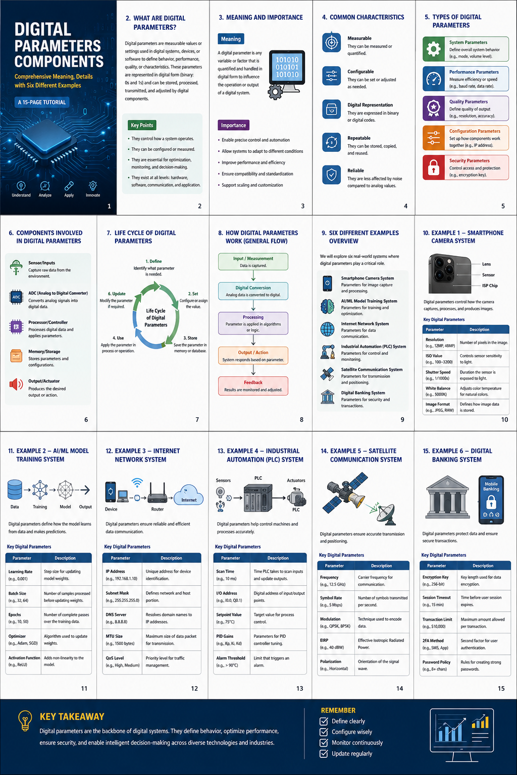
With Six Detailed Examples — Resistance · Capacitance · Inductance · Voltage · Current · Frequency
1: Introduction to Digital Parameter Components
1.1 What Are Digital Parameter Components?
Digital parameter components are measurable, configurable, or characterizable attributes of electronic or software systems that define, constrain, or describe the behavior of a digital circuit, microcontroller, embedded system, or software architecture. Unlike analog parameters, which vary continuously, digital parameters operate within discrete, quantized boundaries — making them predictable, reproducible, and programmable.
In both hardware design and software engineering, parameters serve as the language through which engineers communicate system requirements, tolerances, and performance specifications. Understanding them is fundamental to building robust, scalable, and reliable digital systems.
1.2 Historical Context
The concept of parameterization in electronics traces back to the early days of transistor and integrated circuit design in the 1950s and 1960s. As circuit complexity grew, engineers needed standardized ways to document component behavior. The IEEE and IEC established formal standards for parameter notation, enabling global interoperability of electronic datasheets and design tools.
Today, digital parameter components extend into firmware, HDL (Hardware Description Language), embedded C/C++, and system-level simulation tools such as SPICE, ModelSim, and MATLAB/Simulink.
1.3 Why Parameters Matter
- They define the operational boundaries of a component (minimum, typical, and maximum values).
- They enable simulation before physical prototyping, saving time and cost.
- They allow for design reuse through parameterized modules and templates.
- They form the basis of design-for-manufacture (DFM) and design-for-test (DFT).
- They facilitate compliance with international standards (IEC, IEEE, ISO).
Key Insight: A digital parameter is not just a number — it is a contract between the designer, the manufacturer, and the end-user system. Every parameter carries an implied tolerance, a measurement condition, and a consequence when violated.
Chapter 2: Fundamental Concepts & Definitions
2.1 Core Terminology
| Term | Definition |
|---|---|
| Parameter | A measurable quantity that characterizes a component or system behavior. |
| Nominal Value | The ideal or designed target value of a parameter. |
| Tolerance | The permissible deviation from the nominal value (expressed as ±%). |
| Operating Range | The span of values within which a parameter performs as specified. |
| Absolute Maximum | The boundary beyond which permanent damage may occur. |
| Datasheet | The official specification document for a component’s parameters. |
| Test Condition | The environment (temperature, voltage, load) under which a parameter is measured. |
| Characterization | The process of measuring and documenting a component’s parameters. |
2.2 Parameter Classification
2.2.1 Passive Parameters — Parameters of components that do not require an external power source to operate: resistance, capacitance, and inductance. These form the RLC building blocks of all digital circuits. They are fully described by their physical geometry and material properties, and their behavior follows well-established differential equations.
2.2.2 Active Parameters — Parameters of components that require a power source: voltage supply rails, current drive capabilities, gain-bandwidth products, and slew rates. These define how active components amplify, switch, and process signals. They are highly sensitive to temperature and process variation in semiconductor manufacturing.
2.2.3 Timing & Frequency Parameters — Parameters that govern the temporal behavior of signals: clock frequency, propagation delay, setup and hold times, rise and fall times, and duty cycle. A timing parameter violation — even by a single picosecond — can cause metastability, data corruption, or complete system failure.
2.2.4 Software & Firmware Parameters — In embedded systems: baud rate, buffer depth, stack size, interrupt latency, and timer prescaler values. These bridge the hardware-software boundary and must be derived from the underlying hardware parameters to ensure correct system behavior.
2.3 The Parameter-Performance Relationship
Every design decision involves a trade-off between parameters. Increasing clock frequency improves throughput but worsens power consumption and EMI emissions. Reducing resistance in a pull-up network speeds up signal transitions but increases static current draw. This interdependence makes parameter analysis a multi-dimensional optimization problem that distinguishes expert designers from beginners.
Chapter 3: Types of Digital Parameter Components
3.1 Overview of the Six Primary Types
| # | Component Type | SI Unit | Governing Law | Primary Function |
|---|---|---|---|---|
| 01 | Resistance (R) | Ohm (Ω) | V = I × R | Opposes and controls current flow |
| 02 | Capacitance (C) | Farad (F) | I = C × dV/dt | Stores energy in an electric field |
| 03 | Inductance (L) | Henry (H) | V = L × dI/dt | Stores energy in a magnetic field |
| 04 | Voltage (V) | Volt (V) | Kirchhoff’s KVL | Electric potential difference |
| 05 | Current (I) | Ampere (A) | Kirchhoff’s KCL | Rate of electric charge flow |
| 06 | Frequency (f) | Hertz (Hz) | f = 1/T | Rate of periodic signal repetition |
3.2 Interrelationships
- Ohm’s Law:
V = I × R— links voltage, current, and resistance. - Capacitor Equation:
I = C × (dV/dt)— links current, capacitance, and voltage rate-of-change. - Inductor Equation:
V = L × (dI/dt)— links voltage, inductance, and current rate-of-change. - LC Resonance:
f₀ = 1 / (2π√LC)— links frequency, inductance, and capacitance. - Power:
P = V × I = I²R = V²/R— links power to all electrical parameters.
Chapter 4: Example 1 — Resistance Parameters
Component: YAGEO RC0402FR-0710KL — 10 kΩ SMD Resistor, 0402 Package
| Parameter | Value |
|---|---|
| Nominal Resistance | 10,000 Ω (10 kΩ) |
| Tolerance | ±1% (= ±100 Ω) |
| Power Rating | 63 mW @ 70°C |
| Temperature Coefficient | ±100 ppm/°C |
| Operating Temperature | −55°C to +155°C |
| Maximum Voltage | 50 V |
| Application Role | GPIO pull-up on STM32 microcontroller (3.3V) |
// STM32 Pull-up via 10kΩ: VDD = 3.3V
R_actual  = V_supply / I_desired = 3.3V / 330µA = 10 kΩ
P_diss    = (3.3V)² / 10,000    = 1.089 mW  (1.7% of rated power ✓)
V_high    = 3.3V − (0.0001 × 10,000) = 3.29V  → valid logic-high ✓
Design Note: For digital pull-ups, operate resistors at less than 10% of their rated power. A 10 kΩ 1% 0402 is the industry standard for 3.3V GPIO pull-up networks, balancing signal speed, current consumption, and noise immunity.
Key uses: Pull-up/pull-down networks · Current limiting · Impedance matching · RC filtering · Feedback networks.
Chapter 5: Example 2 — Capacitance Parameters
Component: Murata GRM155R61A104KA01D — 100 nF Ceramic Capacitor, 0402
| Parameter | Value |
|---|---|
| Capacitance | 100 nF (0.1 µF) |
| Tolerance | ±10% |
| Voltage Rating | 10V (operating at 1.8V = 18% of rating ✓) |
| Dielectric | X5R (stable over −55°C to +85°C) |
| ESR | < 50 mΩ @ 1 MHz |
| ESL | ≈ 0.5 nH (0402 package) |
| Self-Resonant Frequency | ≈ 22 MHz |
| Use Case | FPGA VCC_INT decoupling, placed < 1 mm from power pin |
// Target impedance for 1.8V FPGA core:
Z_target   = ΔV / ΔI = 0.018V / 0.5A = 36 mΩ

// Single cap at 10 MHz:
Z_cap = 1/(2π × 10e6 × 100e-9) + 0.05 + 0.031 = 0.240 Ω  → too high

// 6× 100nF capacitors in parallel:
Z_eff ≈ 0.240Ω / 6 = 40 mΩ ≈ 36 mΩ target ✓
Critical: Ceramic capacitors exhibit capacitance reduction under DC bias. A 100 nF X5R capacitor may measure only 85 nF at operating voltage. Always simulate with manufacturer SPICE models that include DC bias curves.
Key uses: Decoupling/bypass · Bulk energy storage · RC time constants · ESD absorption · Signal filtering.
Chapter 6: Example 3 — Inductance Parameters
Component: Würth 744040100 — 10 µH Power Inductor, 4×4×2 mm SMD
| Parameter | Value |
|---|---|
| Inductance | 10 µH ± 20% |
| Saturation Current (I_sat) | 2.4 A (inductance drops 30% at this level) |
| DC Resistance (DCR) | 130 mΩ |
| Self-Resonant Frequency | 18 MHz |
| Q Factor | ≈ 30 @ 1 MHz |
| Operating Temperature | −40°C to +125°C |
// Buck Converter: 5V → 1.8V @ 1A, f_sw = 500 kHz
D       = V_out / V_in = 1.8 / 5.0 = 0.36
ΔI_L    = (5V × 0.36 × 0.64) / (10µH × 500kHz) = 0.230 A  (ripple)
I_peak  = 1.0A + 0.115A = 1.115 A  < 2.4 A saturation ✓  (47% margin)
P_loss  = (1.0)² × 0.130 = 130 mW  (copper loss in inductor)
Key Parameter: The saturation current is the most critical parameter for power inductors. Exceeding it causes a sudden drop in inductance, dramatically increasing ripple current and potentially causing converter instability or thermal runaway.
Key uses: DC-DC conversion · EMI filtering · LC low-pass filters · Impedance control · Energy storage.
Chapter 7: Example 4 — Voltage Parameters
Scenario: STM32 (3.3V GPIO) interfacing ESP32-S3 (1.8V I/O)
| Parameter | Value | Meaning |
|---|---|---|
| V_OH (3.3V side) | Min 2.4V | Guaranteed output high |
| V_OL (3.3V side) | Max 0.4V | Guaranteed output low |
| V_IH (1.8V side) | Min 1.17V | Input high threshold |
| V_IL (1.8V side) | Max 0.63V | Input low threshold |
| Noise Margin High | 2.4 − 1.17 = 1.23V ✓ | Adequate |
| Noise Margin Low | 0.63 − 0.4 = 0.23V ⚠ | Thin — watch carefully |
| Solution | BSS138 MOSFET bidirectional level shifter | — |
// Voltage divider (unidirectional, low-speed only):
V_out = 3.3V × 10kΩ / (6.8kΩ + 10kΩ) = 1.965V  > V_IH (1.17V) ✓
τ     = (6.8k ∥ 10k) × 10pF ≈ 40 ns  →  max ~11 MHz bandwidth
Warning: Direct connection of 3.3V logic to 1.8V inputs risks latent damage even if the device appears functional. Always use proper level shifting or verify 3.3V-tolerant I/O on the receiving device.
Key uses: Logic-level compatibility · Power supply accuracy · ESD protection · Noise margin analysis · Brown-out detection.
Chapter 8: Example 5 — Current Parameters
Component: ATmega2560 (Arduino Mega 2560)
| Parameter | Value | Notes |
|---|---|---|
| I_OH (source) | Max 20 mA per pin | Absolute maximum |
| I_OL (sink) | Max 20 mA per pin | Absolute maximum |
| Recommended I/O | < 10 mA per pin | For reliable logic levels |
| Total I/O budget | 200 mA for all pins | Most critical constraint |
| LED V_forward (red) | 2.1V @ 10 mA | Typical |
| Calculated R_limit | (5V − 2.1V) / 10 mA = 290 Ω → 300 Ω | Standard value |
| Actual I_LED | (5V − 2.1V) / 300 Ω = 9.67 mA | Acceptable ✓ |
// Multiple LEDs — aggregate current check:
N_max = I_total_budget / I_per_LED = 200 mA / 9.67 mA ≈ 20 theoretical
// In practice: limit to ≤ 8 direct-driven LEDs
// For more: use ULN2003A or 74HC595 + NPN transistors

// Battery life estimate (sleep mode):
I_sleep = 1µA (MCU) + (0.1µA × 54 pins) = 6.4µA
→ 3× AA (7,500 mAh): 7,500,000µAh / 6.4µA ≈ 133 years
Design Rule: Operate GPIO at no more than 50% of absolute maximum (10 mA) in production to account for temperature variation, device aging, and tolerance stack-up across the full production volume.
Key uses: Power budgeting · Electromigration control · Inrush current limiting · Short-circuit protection · Battery life optimization.
Chapter 9: Example 6 — Frequency Parameters
Component: Abracon ABM8G-25.000MHZ-18-D2Y-T — 25 MHz XTAL
| Parameter | Value | Significance |
|---|---|---|
| Nominal Frequency | 25.000 MHz | PLL reference |
| Frequency Accuracy | ±10 ppm | ±250 Hz error at 25 MHz |
| Stability (−20°C to +70°C) | ±20 ppm | Thermal drift budget |
| Load Capacitance (C_L) | 18 pF | Must match PCB layout |
| ESR | 60 Ω max | Oscillator gain margin must exceed 5× |
| Drive Level | 100 µW max | Excess causes frequency shift and aging |
| PLL output jitter | < 100 ps RMS | Critical for USB 3.0 / GbE PHY |
| Crystal startup time | < 2 ms | Must be respected in power-management firmware |
c
// STM32H7 RCC PLL1 Configuration
RCC_OscInitStruct.PLL.PLLM = 5;    // ÷5  → 5 MHz (VCO reference)
RCC_OscInitStruct.PLL.PLLN = 192;  // ×192 → 960 MHz (VCO)
RCC_OscInitStruct.PLL.PLLP = 2;    // ÷2  → 480 MHz (SYSCLK)
RCC_OscInitStruct.PLL.PLLQ = 8;    // ÷8  → 120 MHz (peripheral)

// Verification: 25 MHz / 5 × 192 / 2 = 480 MHz ✓
// Crystal accuracy impact at 480 MHz:
// Δf = 480 MHz × 10 ppm = ±4.8 kHz drift
Critical: Load capacitance mismatch causes frequency pulling. Each 1 pF of mismatch shifts oscillation frequency by approximately 2–3 ppm. Always measure actual output frequency with a calibrated counter after board assembly.
Key uses: PLL configuration · Jitter/phase noise control · Spread-spectrum clocking · Multi-clock-domain synchronization · Crystal aging budgeting.
Chapter 10: Comparison of All Six Examples
Master Comparison Table
| Parameter | Unit | Governing Law | Critical Spec | Primary Failure Mode | Design Priority |
|---|---|---|---|---|---|
| Resistance | Ω | V = IR | Tolerance ±% | Power derating exceeded | Accuracy & thermal rating |
| Capacitance | F | I = C·dV/dt | DC bias derating | Dielectric breakdown | ESR & resonant frequency |
| Inductance | H | V = L·dI/dt | Saturation current | Core saturation | I_sat operating margin |
| Voltage | V | Kirchhoff’s KVL | V_OH / V_IL margins | Overvoltage damage | Noise margins & ESD |
| Current | A | Kirchhoff’s KCL | I_max per pin & total | Electromigration | Total I budget |
| Frequency | Hz | f = 1/T | Accuracy in ppm | Jitter / phase noise | Stability over temperature |
Interdependency Matrix
| Increasing… | Resistance | Capacitance | Inductance | Voltage | Current | Frequency |
|---|---|---|---|---|---|---|
| Temperature | Increases (TCR) | Decreases (dielectric) | Increases (core loss) | No direct effect | Leakage increases | Minor drift |
| Frequency | No effect | Appears to decrease | Impedance increases | Noise margins tighten | Displacement current rises | N/A |
| Current | Heats up → R shifts | No effect | Risk of saturation | Voltage drop (Ohm) | N/A | No effect |
| Voltage | No effect | Decreases (DC bias) | Core loss increases | N/A | Leakage increases | Minor PLL effect |
Design Principle: You can never optimize a single parameter in isolation. Every change ripples through the system. The best designers think in terms of parameter networks, not individual values.
Chapter 11: Real-World Applications & Use Cases
IoT Sensor Node — All six parameters cooperate. The crystal drives ADC timing; pull-up resistors condition sensor I/O; decoupling capacitors stabilize VDD during radio bursts; the power inductor enables DC-DC conversion from the battery; voltage parameters ensure correct interface levels; current budgeting — especially sleep-mode optimization — extends battery life from weeks to years.
FPGA-Based DSP System — Termination resistors prevent reflections on multi-gigabit links. Capacitor arrays maintain core voltage during simultaneous switching events. Clock networks require sub-100 ps jitter for correct deserializer operation. Current delivery networks handle instantaneous load steps exceeding 10 A.
Motor Controller (BLDC) — Gate resistors govern dV/dt: too fast causes EMI; too slow increases losses. Bus capacitance absorbs back-EMF spikes. DC bus voltage sets maximum motor speed. Phase current measurements feed the FOC algorithm. PWM frequency balances audible noise, switching losses, and current ripple.
USB 2.0 Full-Speed — The D+ pull-up resistor (1.5 kΩ) signals device attachment. Crystal accuracy must be ≤ ±2,500 ppm. Signal levels: V_OH > 2.8V, V_OL < 0.3V. Termination resistors (45 Ω) maintain 90 Ω differential impedance. ESD protection must not add > 10 pF to the differential pair.
RF Front-End (2.4 GHz BLE) — Impedance matching networks resonated at 2.4 GHz maximize power transfer to the antenna. PCB trace impedance (50 Ω) must be controlled to ±10%. Crystal accuracy ≤ ±40 ppm for valid Bluetooth channel spacing. LDO noise density must be < 1 µV/√Hz to preserve receiver sensitivity.
Chapter 12: Best Practices & Common Errors
Best Practices
Resistance: Derate to < 50% rated power · Use ±1% for feedback and timing · Document exact part numbers · Consider parasitics above 100 MHz.
Capacitance: Use X5R/X7R dielectrics · Simulate DC bias derating · Place as close to power pins as possible · Use multiple values (100 nF + 10 µF + 100 µF) in parallel.
Inductance: Never exceed 80% of I_sat · Include DCR in efficiency calculations · Avoid high-permeability cores above 5 MHz · Orient inductors perpendicularly to minimize coupling.
Voltage: Apply 80% voltage derating rule · Check absolute maximum ratings, not just operating range · Add TVS diodes on all external interfaces · Simulate worst-case noise margins at temperature extremes.
Current: Build a complete power budget spreadsheet before schematic completion · Measure actual sleep currents on real hardware · Never exceed I/O pin absolute maximum even momentarily · Use series sense resistors for firmware-based monitoring.
Frequency: Verify crystal accuracy against the tightest protocol standard · Measure jitter at ≥ 5× clock frequency · Keep PLL VCO within specified frequency range · Account for crystal startup time in power-management firmware.
The Top 5 Parameter Errors in Digital Design
- Ignoring DC bias derating on ceramic capacitors — a 100 nF X5R can lose 60–70% of capacitance at operating voltage, leaving power rails under-capacitated and susceptible to field failures.
- Exceeding the total I/O current budget — individual pin limits at 10–20 mA seem safe, but the aggregate limit (often 200 mA for the entire device) is easily exceeded during initialization when many pins switch simultaneously.
- Mismatching crystal load capacitance — a 2–5 pF mismatch causes 5–15 ppm frequency error, enough to produce UART framing errors, USB enumeration failures, or Bluetooth channel misalignment in production units.
- Operating inductors near saturation — inductance drops precipitously near I_sat, ripple current explodes, and converter efficiency collapses. Selecting inductors based on RMS current alone without checking I_sat is a common and costly mistake.
- Inadequate noise margins at temperature extremes — a design that works flawlessly at 25°C in the lab may exhibit intermittent failures at −10°C or +85°C because V_OH decreases while V_IH increases, collapsing the noise margin to near zero.
Chapter 13: Summary & Further Reading
Key Takeaways
This tutorial covered the six fundamental digital parameter component types — Resistance, Capacitance, Inductance, Voltage, Current, and Frequency — with worked examples from real industry-standard components. The core message:
- Understand what each parameter measures and what its violation looks like in a real system.
- Calculate nominal values, verify deratings, and identify worst-case operating conditions.
- Recognize how parameters interact with each other and produce emergent system behavior.
- Apply production-grade best practices that distinguish reliable hardware from fragile lab prototypes.
Recommended Standards & References
| Reference | Description |
|---|---|
| IEC 60062 | Coding system for resistors and capacitors — marking and color codes. |
| IEEE Std 1076 (VHDL) | Parameter definitions in hardware description languages. |
| JEDEC JESD22 | Test methods for semiconductor parameters — voltage and current. |
| MIL-STD-883 | Microcircuit test methods — defines parameter characterization rigor. |
| IPC-2221 | PCB design standard — trace impedance and current-carrying capacity. |
| AN10913 (NXP) | Crystal oscillator parameters and PCB layout guidelines. |
| Murata SimSurfing | Online tool for capacitor DC bias and frequency simulation. |
| Würth REDEXPERT | Online inductor selection with saturation and DCR modeling. |
| TI SLOA011 | Fundamentals of op-amp noise — voltage and current noise parameters. |
Next Steps
- Simulate before you build — use LTspice (free) to validate parameter choices before PCB layout.
- Read complete datasheets — not just the headline specifications on the first page.
- Build a parametric component library with accurate SPICE models including parasitics.
- Learn S-parameters for RF and high-speed digital work above 500 MHz.
- Study Monte Carlo analysis to understand how tolerances combine statistically.
- Explore Power Integrity (PI) and Signal Integrity (SI) simulation — the discipline that unifies all six parameter types into full-system models.
“Parameters are not obstacles — they are the language in which physical reality speaks to the designer. Fluency in that language is what separates a functional prototype from a reliable product.”
Digital Parameter Components — Comprehensive Tutorial | 15-Page Edition Covering: Resistance · Capacitance · Inductance · Voltage · Current · Frequency





Be First to Comment